Spinning around: A room temperature field-effect transistor using graphene's electron spin
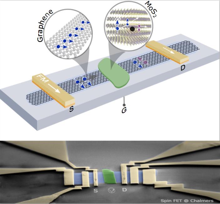
This is a schematic of graphene-MoS2 heterostructure which allows spin injection into graphene from the ferromagnetic source, diffusive spin transport in the graphene-MoS2 heterostructure channel, spin manipulation by a gate voltage and detection of spin signal by the ferromagnetic drain. Credit: Spin FET@Chalmers
Current semiconductor logic devices within our computers use the flow and control of electronic charge for information processing. Spintronic memory devices use the intrinsic properties of electron spin to store information. For future devices, researchers are searching for ways to integrate both information processing and storage in one device unit.
“Graphene is an excellent medium for spin transport at room temperature, due to its low atomic mass. However, an unsolved challenge was to control the spin current at ambient temperature” explains Saroj Dash, group leader and Associate Professor at Chalmers University of Technology.
The Graphene Flagship researchers Andre Dankert and Saroj Dash have now shown that it is possible to electrically manipulate the spin properties of graphene in a controlled manner at room temperature. This not only could open many new possibilities in spin logic operations but also integration with magnetic memory elements in a single device. With further developments, if one could produce a spin current without charge flow, this will require far less power and lead to more versatile devices. This is especially important as we move more and more toward hand held mobile computing.
“Controlling the flow of spin currents in a transistor-like manner is a decade old dream and the missing link towards all-electrical spin logic applications.” says the lead author Andre Dankert from Chalmers University of Technology, “Researchers were working for almost ten years to understand the spin transport properties of various layered materials and how they can be tuned to achieve this goal. Our work is an important milestone in the field of spintronics.”
Graphene has been shown to transport spin over long distances by several Flagship Groups. Combining graphene with another layered material where spin lasts much less time can produce a spin field-effect transistor like device.
Talking about creating spintronic devices using a heterostructure is Saroj Dash, “By combining graphene, where spin lasts for nano seconds with molybdenum disulfide where spin only lasts for picoseconds you can control where the spin can go by using a gate voltage – essentially you can create a spin switch. Importantly, we show in this research a particular materials mix which enables this spin-switch to work at room temperature.”
Saroj Dash also added “We have been working on graphene spintronics for a number of years and we joined the Graphene Flagship because our goals are aligned with that of the Flagship spintronics work package — to investigate room temperature graphene spintronics devices, joining together theoretical and experiment research. The collaborative nature of the Graphene Flagship community, with its focus on face to face meetings has lead to many fruitful discussions within our spintronics field. This collaborative approach also led to a great relationship with our commercial partner Graphenea, who has worked with us to provide the graphene sample we needed.”
Speaking about the next steps in his research Andre Dankert said, “Now we know the crucial parameters of our device structure, we can optimise it to increase the effective gain and transistor action.”
Many layered materials are promising for spintronics. In addition to exploring the interesting properties of these individual crystals, it is intriguing to reveal the potential of their heterostructures. The bigger goal is to create novel spin phenomena in layered materials based devices by stacking different layers with complementary properties, Saroj Dash explained.
Bart van Wees, leader of the spintronics work package adds, “The future challenge will be to explore and use the new spintronic functionalities which are made possible by the new van der Waals heterostructures. The authors already made an important step here.”
Professor Andrea Ferrari, Chair of the Management Panel and Science and Technology Officer of the Graphene Flagship added: “spintronics has been one of the fundamental work packages since the start of the Flagship. It was always seen as a long term investment. It is exciting to see that so much progress has been made towards devices”
###
For further reading on spintronic devices please see this 2013 Graphene Flagship piece: From Science to Technology, Graphene Spintronics.
Media Contact
All latest news from the category: Physics and Astronomy
This area deals with the fundamental laws and building blocks of nature and how they interact, the properties and the behavior of matter, and research into space and time and their structures.
innovations-report provides in-depth reports and articles on subjects such as astrophysics, laser technologies, nuclear, quantum, particle and solid-state physics, nanotechnologies, planetary research and findings (Mars, Venus) and developments related to the Hubble Telescope.


Newest articles
Peptides on Interstellar Ice
A research team led by Dr Serge Krasnokutski from the Astrophysics Laboratory at the Max Planck Institute for Astronomy at the University of Jena had already demonstrated that simple peptides…
A new look at the consequences of light pollution
GAME 2024 begins its experiments in eight countries. Can artificial light at night harm marine algae and impair their important functions for coastal ecosystems? This year’s project of the training…

Silicon Carbide Innovation Alliance to drive industrial-scale semiconductor work
Known for its ability to withstand extreme environments and high voltages, silicon carbide (SiC) is a semiconducting material made up of silicon and carbon atoms arranged into crystals that is…

