Scientists Image 'Magnetic Semiconductors' On The Nanoscale

The findings, scheduled for publication as the cover story of the July 27 issue of the journal Nature, bring scientists one step closer toward realizing the goal of building a very advanced semiconductor computer chip. The chip would be based upon a property of the electron called “spin” and the related technology of “spintronics,” according to Michael Flatté, professor in the UI College of Liberal Arts and Sciences Department of Physics and Astronomy.
“With spintronics, data manipulation and long-term storage can be conducted in one computer chip, rather than separately in a CPU and a hard drive as currently practiced. The data manipulation could also be done quicker and require less power. Such a computer would be much smaller in size and use less energy,” Flatté says.
He adds that some 20 years ago, researchers at IBM discovered that an ordinary semiconducting material, indium arsenide, could be made magnetic at low temperatures by introducing a very small number of magnetic atoms. The magnetic atoms they added were manganese, and soon many other “magnetic semiconductors” were discovered. Gallium arsenide, a semiconductor material used for high-performance devices in cell phones, becomes magnetic when manganese is added, but only at a temperature of -88 C (-126 F). In order for it to be used in future computer chips, magnetic semiconductors like gallium manganese arsenide must remain magnetic at higher temperatures and also be made “cleaner,” or less resistant to current flow.
“Visualizing the magnetic interactions on the nanoscale may lead to better magnetic semiconductor materials and applications for them in the electronics industry,” says Flatté, who along with UI Assistant Research Scientist Jian-Ming Tang predicted that the magnetic interactions could be imaged with a scanning tunneling microscope. “An electron behaves as if it carries a small magnet around with it. This property, called “spin,” has not been used in computer chips to date. If the materials are good enough, then new computer chips that require much less power to run are possible. Even revolutionary 'quantum computers' that use strange quantum phenomena of the atomic world to perform calculations may be possible,” says Flatté.
Flatté and Tang had predicted that the magnetic interactions should depend strongly on where in the crystal lattice of the semiconductor the atoms were sitting. Some configurations interacted very strongly and others very weakly. “We thought it would require a lot of luck to see this effect. Usually when manganese is placed in gallium arsenide, it enters the lattice in many different positions. To see two manganese atoms within a nanometer of each other, but isolated from all other manganese, would be statistically very unlikely,” he says.
Flatté and Tang, theorists, teamed up with experimentalists Professor Ali Yazdani, Dale Kitchen and Anthony Richardella to look for these effects. The experimentalists took a completely different approach toward seeing the magnetic interactions. Instead of trusting luck to help them find an arrangement of atoms, they placed the manganese atoms one at a time into a fresh, clean piece of gallium arsenide. “Using the tip of a scanning tunneling microscope, we can take out a single atom from the base material and replace it with a single metal that gives the semiconductor its magnetic properties,” says Yazdani, Princeton University physics professor. He notes that the effort marks the first time that scientists have achieved this degree of control over the atomic-level structure of a semiconductor. In essence, the team used this unique capability to make a semiconductor magnetic, one atom at a time. “The ability to tailor semiconductors on the atomic scale is the holy grail of electronics, and this method may be the approach that is needed,” says Yazdani.
Kitchen, a researcher in Yazdani's lab, hit upon the solution while working with a high-tech tool used to explore complex materials called a scanning tunneling microscope, a device that operates very differently from a desktop optical microscope. The device has a finely-pointed electrical probe that passes over a surface in order to detect variations with a weak electric field. The team, however, found that the charged tip could also be used to eject a single gallium atom from the surface, replacing it with one of manganese that was waiting nearby.
By incorporating manganese atoms into the gallium arsenide semiconductor, the team has created an atomic-scale laboratory that can reveal what researchers have sought for decades: the precise interactions among atoms and electrons in chip materials. The team used their new technique to find the optimal arrangements for manganese atoms that enhance the magnetic properties of gallium manganese arsenide. These arrangements agreed with Flatté and Tang's predictions. “To predict how a material will behave, and then have that prediction dramatically confirmed, as in this experiment, is one of the most enjoyable experiences of research,” says Flatté.
Flatté cautions that further advances will be required to translate the new research results into new chip technology and also that using a scanning tunneling microscope to grow large pieces of high quality gallium manganese arsenide may not be practical. However, he says, the lessons learned about optimal arrangements of magnetic atoms in semiconductors will be transferred to other semiconductor growth techniques and to other magnetic semiconductor materials.
The research project was funded in part by the National Science Foundation and the U.S. Army Research Office.
STORY SOURCE: University of Iowa News Services, 300 Plaza Centre One, Suite 371, Iowa City, Iowa 52242-2500.
MEDIA CONTACT: Gary Galluzzo, 319-384-0009, gary-galluzzo@uiowa.edu
Media Contact
More Information:
http://www.uiowa.eduAll latest news from the category: Physics and Astronomy
This area deals with the fundamental laws and building blocks of nature and how they interact, the properties and the behavior of matter, and research into space and time and their structures.
innovations-report provides in-depth reports and articles on subjects such as astrophysics, laser technologies, nuclear, quantum, particle and solid-state physics, nanotechnologies, planetary research and findings (Mars, Venus) and developments related to the Hubble Telescope.
Newest articles

Properties of new materials for microchips
… can now be measured well. Reseachers of Delft University of Technology demonstrated measuring performance properties of ultrathin silicon membranes. Making ever smaller and more powerful chips requires new ultrathin…

Floating solar’s potential
… to support sustainable development by addressing climate, water, and energy goals holistically. A new study published this week in Nature Energy raises the potential for floating solar photovoltaics (FPV)…

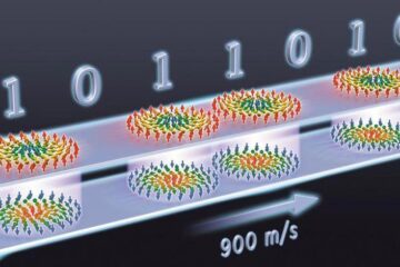
Skyrmions move at record speeds
… a step towards the computing of the future. An international research team led by scientists from the CNRS1 has discovered that the magnetic nanobubbles2 known as skyrmions can be…


