Growing glowing nanowires to light up the nanoworld
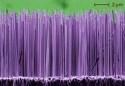
Growing, glowing nanowires. Credit: Lorelle Mansfield/NIST
The nano world is getting brighter. Nanowires made of semiconductor materials are being used to make prototype lasers and light-emitting diodes with emission apertures roughly 100 nm in diameter–about 50 times narrower than conventional counterparts. Nanolight sources may have many applications, including “lab on a chip” devices for identifying chemicals and biological agents, scanning-probe microscope tips for imaging objects smaller than is currently possible, or ultra-precise tools for laser surgery and electronics manufacturing.
Researchers at the National Institute of Standards and Technology (NIST) are growing nanowires made of gallium nitride alloys and making prototype devices and nanometrology tools. The wires are grown under high vacuum by depositing atoms layer by layer on a silicon crystal. NIST is one of few laboratories capable of growing such semiconductor nanowires without using metal catalysts, an approach believed to enhance luminescence and flexibility in crystal design. The wires are generally between 30 and 500 nanometers (nm) in diameter and up to 12 micrometers long. When excited with a laser or electric current, the wires emit an intense glow in the ultraviolet or visible parts of the spectrum, depending on the alloy composition.
A paper in the May 22 issue of Applied Physics Letters* reports that individual nanowires grown at NIST produce sufficiently intense light to enable reliable room-temperature measurements of their important characteristics. For example, the peak wavelength of light emitted with electric field parallel to the long axis of a nanowire is shifted with respect to the peak wavelength emitted with electric field perpendicular to the wire. Such differences in emission are used to characterize the nanowire materials and also may be exploited to make sensors and other devices.
NIST has grown a variety of nanowires and extensively characterized their structural and optical properties, finding few defects, strains or impurities, which results in high light output compared to the bulk material.** The wires also can be transferred from the silicon crystal to other substrates, such as sapphire, and arranged using electric fields. The NIST team has used the nanowires to make a number of prototype devices, including light-emitting diodes, field-effect transistors, and nanowire “bridge” structures that may be useful in sensors and nanoscale mechanical resonators.
Media Contact
More Information:
http://www.nist.govAll latest news from the category: Physics and Astronomy
This area deals with the fundamental laws and building blocks of nature and how they interact, the properties and the behavior of matter, and research into space and time and their structures.
innovations-report provides in-depth reports and articles on subjects such as astrophysics, laser technologies, nuclear, quantum, particle and solid-state physics, nanotechnologies, planetary research and findings (Mars, Venus) and developments related to the Hubble Telescope.


Newest articles

Bringing bio-inspired robots to life
Nebraska researcher Eric Markvicka gets NSF CAREER Award to pursue manufacture of novel materials for soft robotics and stretchable electronics. Engineers are increasingly eager to develop robots that mimic the…

Bella moths use poison to attract mates
Scientists are closer to finding out how. Pyrrolizidine alkaloids are as bitter and toxic as they are hard to pronounce. They’re produced by several different types of plants and are…
AI tool creates ‘synthetic’ images of cells
…for enhanced microscopy analysis. Observing individual cells through microscopes can reveal a range of important cell biological phenomena that frequently play a role in human diseases, but the process of…

