New process builds electronic function into optical fiber
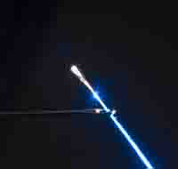
<br>These photos show a glass fiber with a bundle of semiconductor wires emanating from it. Each wire is just 2 microns in diameter--20 times smaller than a human hair. The glass fiber is glowing from blue laser light. One of the images shows the wire-packed glass fiber passing through the eye of a needle. Credit: Neil Baril, Penn State.
Optical fiber helped bring us the Internet, and silicon/germanium devices brought us microelectronics. Now, a joint team from Penn State University and the University of Southampton has developed a new way to combine these technologies. The team has made semiconductor devices, including a transistor, inside microstructured optical fibers. The resulting ability to generate and manipulate signals inside optical fibers could have applications in fields as diverse as medicine, computing, and remote sensing devices.
Optical fiber has proved to be the ideal medium for transmitting signals based on light, while crystalline semiconductors are the best way to manipulate electrons. One of the greatest current technological challenges is exchanging information between optics and electronics rapidly and efficiently. This new technique may provide the tools to cross the divide. The results of this research will be published in the 17 March edition of the journal Science.
“This advance is the basis for a technology that could build a large range of devices inside an optical fiber,” said John Badding, associate professor of chemistry at Penn State University. While the optical fiber transmits data, a semiconductor device allows active manipulation of the light, including generating and detecting, amplifying signals, and controlling wavelengths. “If the signal never leaves the fiber, then it is faster, cheaper and more efficient,” said Badding. ”
“This fusion of two separate technologies opens the possibility of true optoelectronic devices that do not require conversion between optical and electronic signals,” said Pier Sazio, senior research fellow in the Optoelectronics Research Centre at the University of Southampton (UK). “If you think of the fiber as a water main, this structure places the pumping station inside the pipe. The glass fiber provides the transmission and the semiconductor provides the function.”
Beyond telecommunications, optical fibers are used in a wide range of technologies that employ light. “For example, in endoscopic surgery, by building a laser inside the fiber you might be able to deliver a wavelength that could not otherwise be used,” said Badding.
The key breakthrough was the ability to form crystalline semiconductors that nearly fill the entire inside diameter, or pore, of very narrow glass capillaries. These capillaries are optical fibers–long, clear tubes that can carry light signals in many wavelengths simultaneously. When the tube is filled with a crystalline semiconductor, such as germanium, the semiconductor forms a wire inside the optical fiber. The combination of optical and electrical capabilities provides the platform for development of new optoelectronic devices.
The crystals were formed using chemical vapor deposition (CVD) to deposit germanium and other semiconductors inside the long, narrow pores of the hollow optical fiber. In the CVD process, a germanium compound is vaporized and then forced through the pores of the fiber at pressures as high as 1000 times atmospheric pressure and temperatures up to 500°C. A chemical reaction within the fiber allows germanium to coat the interior walls of the hollow fiber and then form crystals that grow inward. “The process works so perfectly that you can get a germanium tube that has an opening in the center of only 25 nanometers through the length of the fiber,” said Sazio. “This is only a tiny fraction of the diameter of the fiber pore, so it is essentially a wire.” This is the first demonstration of building crystalline structures, which are best for semiconductor devices, inside the pores of the capillaries.
The team has built a simple in-fiber transistor, and they point to the success of the Erbium Doped Fiber Amplifier, which was invented at Southampton in the late 1980s, to illustrate the transformational possibilities of this technology. By incorporating the chemical element erbium into the fiber, the Erbium Amplifier allows efficient transmission of data signals in transoceanic optical fibers. “Without that kind of device, it would be necessary to periodically convert the light to an electronic signal, amplify the signal, and convert it back to light, which is expensive and inefficient” said Sazio. ” Since its inception, the Erbium Amplifier has made the internet possible in its current form.”
Beyond the simple devices that this research has demonstrated, the research team sees the potential for the embedded semiconductors to carry optoelectronic applications to the next level. “At present you still have electrical switching at both ends of the optical fiber,” says Badding. “If we can get to the point where the signal never leaves the fiber, it will be faster and more efficient. If we can actually generate signals inside a fiber, a whole range of optoelectronic applications become possible.”
Media Contact
More Information:
http://www.psu.eduAll latest news from the category: Physics and Astronomy
This area deals with the fundamental laws and building blocks of nature and how they interact, the properties and the behavior of matter, and research into space and time and their structures.
innovations-report provides in-depth reports and articles on subjects such as astrophysics, laser technologies, nuclear, quantum, particle and solid-state physics, nanotechnologies, planetary research and findings (Mars, Venus) and developments related to the Hubble Telescope.


Newest articles
“Nanostitches” enable lighter and tougher composite materials
In research that may lead to next-generation airplanes and spacecraft, MIT engineers used carbon nanotubes to prevent cracking in multilayered composites. To save on fuel and reduce aircraft emissions, engineers…
Trash to treasure
Researchers turn metal waste into catalyst for hydrogen. Scientists have found a way to transform metal waste into a highly efficient catalyst to make hydrogen from water, a discovery that…
Real-time detection of infectious disease viruses
… by searching for molecular fingerprinting. A research team consisting of Professor Kyoung-Duck Park and Taeyoung Moon and Huitae Joo, PhD candidates, from the Department of Physics at Pohang University…

