New design for transistors powered by single electrons
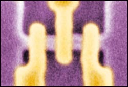
Colorized micrograph of three tunable gates across an electrical channel in a single electron tunneling (SET) transistor.
Scientists have demonstrated the first reproducible, controllable silicon transistors that are turned on and off by the motion of individual electrons. The experimental devices, designed and fabricated at NTT Corp. of Japan and tested at NIST, may have applications in low-power nanoelectronics, particularly as next-generation integrated circuits for logic operations (as opposed to simpler memory tasks).
The transistors, described in the Jan. 30, 2006, issue of Applied Physics Letters,* are based on the principle that as device sizes shrink to the nanometer range, the amount of energy required to move a single electron increases significantly. This makes it possible to control individual electron motion and current flow by manipulating the voltage applied to barriers, or “gates,” in the electrical circuit. At negative voltage, the transistor is off; at higher voltage, the transistor is turned on and individual electrons file through the circuit, as opposed to thousands at a time in a conventional device.
This type of innovative transistor, called a “single-electron tunneling” (SET) device, is typically made with a metal “wire” interrupted by insulating barriers that offer a rigid, narrow range of control over electron flow. Silicon devices, by contrast, have barriers that are electrically “tunable” over a wider operating range, offering finer, more flexible control of the transistor’s on/off switch. Particular voltage levels are applied across the barriers, to manipulate charge, as a means of encouraging or impeding electron flow. Silicon-based devices also allow fabrication using standard semiconductor technology. Until now, however, no silicon SET transistor designs have been reported that are reproducible and controllable.
The NIST/NTT team made five uniform, working silicon transistors with tunable barriers. Each device consists of a silicon channel 360 nanometers (nm) long and 30 nm wide, with three gates crossing the channel. The gates have two levels; the upper level turns the current on and off, while the lower level controls electron flow in small local areas. The team was able to tune gate conductance properties over a wide range, by more than three orders of magnitude.
Media Contact
More Information:
http://www.nist.govAll latest news from the category: Physics and Astronomy
This area deals with the fundamental laws and building blocks of nature and how they interact, the properties and the behavior of matter, and research into space and time and their structures.
innovations-report provides in-depth reports and articles on subjects such as astrophysics, laser technologies, nuclear, quantum, particle and solid-state physics, nanotechnologies, planetary research and findings (Mars, Venus) and developments related to the Hubble Telescope.


Newest articles
Combatting disruptive ‘noise’ in quantum communication
In a significant milestone for quantum communication technology, an experiment has demonstrated how networks can be leveraged to combat disruptive ‘noise’ in quantum communications. The international effort led by researchers…

Stretchable quantum dot display
Intrinsically stretchable quantum dot-based light-emitting diodes achieved record-breaking performance. A team of South Korean scientists led by Professor KIM Dae-Hyeong of the Center for Nanoparticle Research within the Institute for…

Internet can achieve quantum speed with light saved as sound
Researchers at the University of Copenhagen’s Niels Bohr Institute have developed a new way to create quantum memory: A small drum can store data sent with light in its sonic…

