Nanoscientists Provide New Picture of Semiconductor Material

For almost a decade, scientists thought they understood the surface structure of cubic gallium nitride, a promising new crystalline semiconductor. Research by an interdisciplinary team of nanoscientists from Ohio University and the Universitat Autònoma de Barcelona, however, turns that idea on its head.
Their study published in the Sept. 30 online issue of the journal Physical Review Letters provides a fresh – and they argue, more accurate – look at the surface structure of the crystalline material, which could be used in lasers and other electronic devices.
Nancy Sandler, an assistant professor of physics and astronomy at Ohio University, and Pablo Ordejón, a Barcelona professor specializing in the algorithm used in the project, calculated several properties using the currently accepted model and obtained new images of the crystal’s surface. Experimentalists Hamad Al-Brithen and his Ph.D. adviser Arthur Smith, Ohio University associate professor of physics and astronomy, recently had used scanning tunneling microscopy to capture an image of the surface.
When they compared the model image with the experimental image, the researchers found that the theory and the experiment aligned – except for one important detail. Researchers previously thought that the atoms on the surface were arranged in groups of four in one direction but only one in the other. The new finding shows that they are in groups of four in one direction but in groups of three in the other direction, Smith said. The discrepancy calls into question the model scientists have accepted for the last seven years and the understanding of the surface structure.
The surface of the material is not easy to work with, Smith noted, because it’s sensitive to how scientists handle it. A different structure could be created simply by exposing the crystalline surface to other elements. For example, the accidental contact of arsenic (an element commonly used in semiconductor growth) with the crystal surface has affected other researchers’ data in the past.
“The relevance of modeling surfaces is that the ordering of atoms on a surface can be substantially different from the one in the bulk of the material,” Sandler said.
The new research could help scientists learn how to use cubic gallium nitride as a new semiconductor for lasers and other electronic devices such as display technologies and bright blue light-emitting diode (LED) applications. It also may help them grow layers of the material more precisely to create technological applications. But before scientists can make use of this potentially valuable material, they first must understand its basic properties so they can begin tackling its drawbacks, said Smith, director of Ohio University’s Nanoscale and Quantum Phenomena Institute.
“Cubic gallium nitride is more difficult to grow [than the popular hexagonal type of gallium nitride crystal],” said Smith. “But its cubic properties make it more compatible with other commonly used materials, and so it has more potential for integration into mainstream devices.”
The research was supported by grants from the National Science Foundation and Spain’s Ministry of Science and Technology and its Ministry of Education and Science.
This project is the first major paper published by Ohio University’s Nanoscale Interdisciplinary Research Team, a collaboration of researchers funded by the NSF.
Media Contact
More Information:
http://www.ohio.eduAll latest news from the category: Physics and Astronomy
This area deals with the fundamental laws and building blocks of nature and how they interact, the properties and the behavior of matter, and research into space and time and their structures.
innovations-report provides in-depth reports and articles on subjects such as astrophysics, laser technologies, nuclear, quantum, particle and solid-state physics, nanotechnologies, planetary research and findings (Mars, Venus) and developments related to the Hubble Telescope.
Newest articles
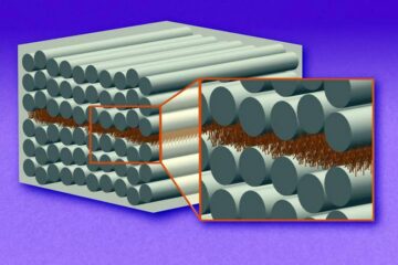
“Nanostitches” enable lighter and tougher composite materials
In research that may lead to next-generation airplanes and spacecraft, MIT engineers used carbon nanotubes to prevent cracking in multilayered composites. To save on fuel and reduce aircraft emissions, engineers…
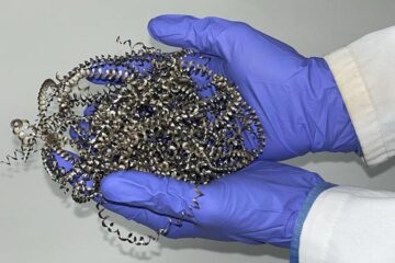
Trash to treasure
Researchers turn metal waste into catalyst for hydrogen. Scientists have found a way to transform metal waste into a highly efficient catalyst to make hydrogen from water, a discovery that…
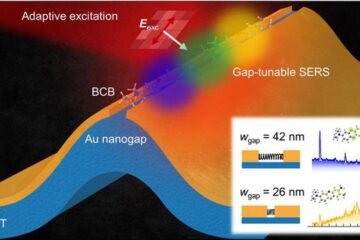
Real-time detection of infectious disease viruses
… by searching for molecular fingerprinting. A research team consisting of Professor Kyoung-Duck Park and Taeyoung Moon and Huitae Joo, PhD candidates, from the Department of Physics at Pohang University…


