NASA Engineer Achieves Another Milestone in Emerging Nanotechnology
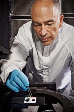
Optics engineer John Hagopian works with a nanotube material sample in this file photograph from NASA's Goddard Space Flight Center in Greenbelt, Md.<br>Image Credit: NASA Goddard/Chris Gunn<br>
A team led by John Hagopian, an optics engineer at NASA’s Goddard Space Flight Center in Greenbelt, Md., has demonstrated that it can grow a uniform layer of carbon nanotubes through the use of another emerging technology called atomic layer deposition or ALD. The marriage of the two technologies now means that NASA can grow nanotubes on three-dimensional components, such as complex baffles and tubes commonly used in optical instruments.
“The significance of this is that we have new tools that can make NASA instruments more sensitive without making our telescopes bigger and bigger,” Hagopian said. “This demonstrates the power of nanoscale technology, which is particularly applicable to a new class of less-expensive tiny satellites called Cubesats that NASA is developing to reduce the cost of space missions.”
Since beginning his research and development effort five years ago, Hagopian and his team have made significant strides applying the carbon-nanotube technology to a number of spaceflight applications, including, among other things, the suppression of stray light that can overwhelm faint signals that sensitive detectors are supposed to retrieve.
Super Absorbency
During the research, Hagopian tuned the nano-based super-black material, making it ideal for this application, absorbing on average more than 99 percent of the ultraviolet, visible, infrared and far-infrared light that strikes it — a never-before-achieved milestone that now promises to open new frontiers in scientific discovery. The material consists of a thin coating of multi-walled carbon nanotubes about 10,000 times thinner than a strand of human hair.
Once a laboratory novelty grown only on silicon, the NASA team now grows these forests of vertical carbon tubes on commonly used spacecraft materials, such as titanium, copper and stainless steel. Tiny gaps between the tubes collect and trap light, while the carbon absorbs the photons, preventing them from reflecting off surfaces. Because only a small fraction of light reflects off the coating, the human eye and sensitive detectors see the material as black.
Before growing this forest of nanotubes on instrument parts, however, materials scientists must first deposit a highly uniform foundation or catalyst layer of iron oxide that supports the nanotube growth. For ALD, technicians do this by placing a component or some other substrate material inside a reactor chamber and sequentially pulsing different types of gases to create an ultra-thin film whose layers are literally no thicker than a single atom. Once applied, scientists then are ready to actually grow the carbon nanotubes. They place the component in another oven and heat the part to about 1,832 F (750 C). While it heats, the component is bathed in carbon-containing feedstock gas.
“The samples we’ve grown to date are flat in shape,” Hagopian explained. “But given the complex shapes of some instrument components, we wanted to find a way to grow carbon nanotubes on three-dimensional parts, like tubes and baffles. The tough part is laying down a uniform catalyst layer. That’s why we looked to atomic layer deposition instead of other techniques, which only can apply coverage in the same way you would spray something with paint from a fixed angle.”
ALD to the Rescue
ALD, first described in the 1980s and later adopted by the semiconductor industry, is one of many techniques for applying thin films. However, ALD offers an advantage over competing techniques. Technicians can accurately control the thickness and composition of the deposited films, even deep inside pores and cavities. This gives ALD the unique ability to coat in and around 3-D objects.
NASA Goddard co-investigator Vivek Dwivedi, through a partnership with the University of Maryland at College Park, is now advancing ALD reactor technology customized for spaceflight applications.
To determine the viability of using ALD to create the catalyst layer, while Dwivedi was building his new ALD reactor, Hagopian engaged through the Science Exchange the services of the Melbourne Centre for Nanofabrication (MCN), Australia’s largest nanofabrication research center. The Science Exchange is an online community marketplace where scientific service providers can offer their services. The NASA team delivered a number of components, including an intricately shaped occulter used in a new NASA-developed instrument for observing planets around other stars.
Through this collaboration, the Australian team fine-tuned the recipe for laying down the catalyst layer — in other words, the precise instructions detailing the type of precursor gas, the reactor temperature and pressure needed to deposit a uniform foundation. “The iron films that we deposited initially were not as uniform as other coatings we have worked with, so we needed a methodical development process to achieve the outcomes that NASA needed for the next step,” said Lachlan Hyde, MCN’s expert in ALD.
The Australian team succeeded, Hagopian said. “We have successfully grown carbon nanotubes on the samples we provided to MCN and they demonstrate properties very similar to those we’ve grown using other techniques for applying the catalyst layer. This has really opened up the possibilities for us. Our goal of ultimately applying a carbon-nanotube coating to complex instrument parts is nearly realized.”
Lori Keesey
NASA's Goddard Space Flight Center, Greenbelt, Md.
Media Contact
All latest news from the category: Physics and Astronomy
This area deals with the fundamental laws and building blocks of nature and how they interact, the properties and the behavior of matter, and research into space and time and their structures.
innovations-report provides in-depth reports and articles on subjects such as astrophysics, laser technologies, nuclear, quantum, particle and solid-state physics, nanotechnologies, planetary research and findings (Mars, Venus) and developments related to the Hubble Telescope.


Newest articles

Properties of new materials for microchips
… can now be measured well. Reseachers of Delft University of Technology demonstrated measuring performance properties of ultrathin silicon membranes. Making ever smaller and more powerful chips requires new ultrathin…

Floating solar’s potential
… to support sustainable development by addressing climate, water, and energy goals holistically. A new study published this week in Nature Energy raises the potential for floating solar photovoltaics (FPV)…

Skyrmions move at record speeds
… a step towards the computing of the future. An international research team led by scientists from the CNRS1 has discovered that the magnetic nanobubbles2 known as skyrmions can be…

