Hybrid Materials For Future Solar Cells

Semiconductor nanocrystals or also called quantum dots exhibit outstanding optical properties compared to organic dyes. Due to the quantum confinement their emission color can be continuously tuned from the ultraviolet to the near infrared range by changing the size and chemical composition.
They exhibit a broad absorption spectrum, a narrow emission band and large absorption cross sections. Their surface can be covered by a few monolayers of different semiconductor materials in such a way that we can either improve their luminescent properties and stability or avoid the fluorescence to obtain charge carriers. The latter effect opens tremendous alternatives in photovoltaics. Due to their optical properties, semiconductor nanoparticles are studied in different disciplines, from optics to biomedicine.
Thanks to a remarkable effort in the synthetic activities in the last 20 years, we can nowadays produce nanoparticles of different materials controlling their size, shape, and surface properties. Examples of nanoparticles produced by non hydrolytic colloidal synthetic methods are CdS, CdTe, InP, GaAs, PbS, or PbSe. However, the most studied system is CdSe, with tunable emission from blue to red. Due to the synthetic approach (hot injection method), the surface of these nanoparticles is capped with an organic shell that protects them and makes them stable in non-polar organic solvents. It is also possible to controllably replace the initial organic shell for water compatible ones. The organic shell plays a relevant role in the quantum efficiency of the nanoparticles and their stability in different media. However, this shell prevents high electrical conduction.
Carbon nanotubes are another example of nanomaterials with extraordinary electrical properties. They consist of one or several rolled up graphene layers. In the case of a single layer they are called single-wall and multi-wall when several layers are rolled-up. Hybrid materials composed of semiconductor nanoparticles and carbon nanotubes combine the high absorption properties of the former and the high electrical conductivity of the latter. One of the main drawbacks in the formation of such hybrid structures focuses on the type of interaction between them. Most of the existing procedures involve the growth of nanoparticles on previous defect sites provoked on the surface or edges of carbon nanotubes by aggressive chemical means. These aggressive treatments render an oxidized nanotube surface or even structural damage that deteriorates their outstanding electrical, mechanical, and optical properties significantly. Thus, supramolecular or electrostatic functionalisations are better approaches for photovoltaic applications.
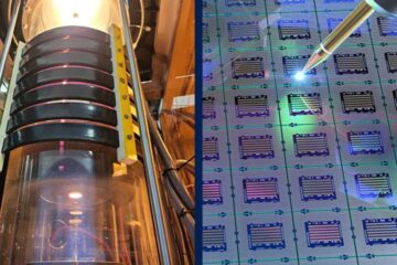
Dr Beatriz H. Juárez, from IMDEA Nanoscience, works on the preparation of hybrid materials with high coverage without modifying the electrical properties of the tubes. Furthermore, the monodispersity of the nanoparticles with high crystallographic quality and a close contact between nanoparticles and nanotubes are also under investigation. The composites show photoelectrical response, injecting charge carriers in the nanotubes upon nanoparticle excitation. Although in an initial stage, the results obtained up to now points out the high potential of these composites to build up photovoltaic devices and solar cells.
B. H. Juárez, C. Klinke, A. Kornowski, H. Weller, Nano Letters, 2007, 7, 3564
Media Contact
More Information:
http://www.imdea.orgAll latest news from the category: Physics and Astronomy
This area deals with the fundamental laws and building blocks of nature and how they interact, the properties and the behavior of matter, and research into space and time and their structures.
innovations-report provides in-depth reports and articles on subjects such as astrophysics, laser technologies, nuclear, quantum, particle and solid-state physics, nanotechnologies, planetary research and findings (Mars, Venus) and developments related to the Hubble Telescope.
Newest articles

Silicon Carbide Innovation Alliance to drive industrial-scale semiconductor work
Known for its ability to withstand extreme environments and high voltages, silicon carbide (SiC) is a semiconducting material made up of silicon and carbon atoms arranged into crystals that is…

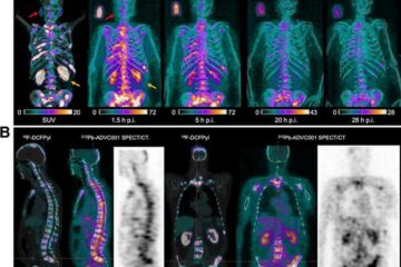
New SPECT/CT technique shows impressive biomarker identification
…offers increased access for prostate cancer patients. A novel SPECT/CT acquisition method can accurately detect radiopharmaceutical biodistribution in a convenient manner for prostate cancer patients, opening the door for more…

How 3D printers can give robots a soft touch
Soft skin coverings and touch sensors have emerged as a promising feature for robots that are both safer and more intuitive for human interaction, but they are expensive and difficult…


