Graphene Research: Electrons Moving along Defined Snake States
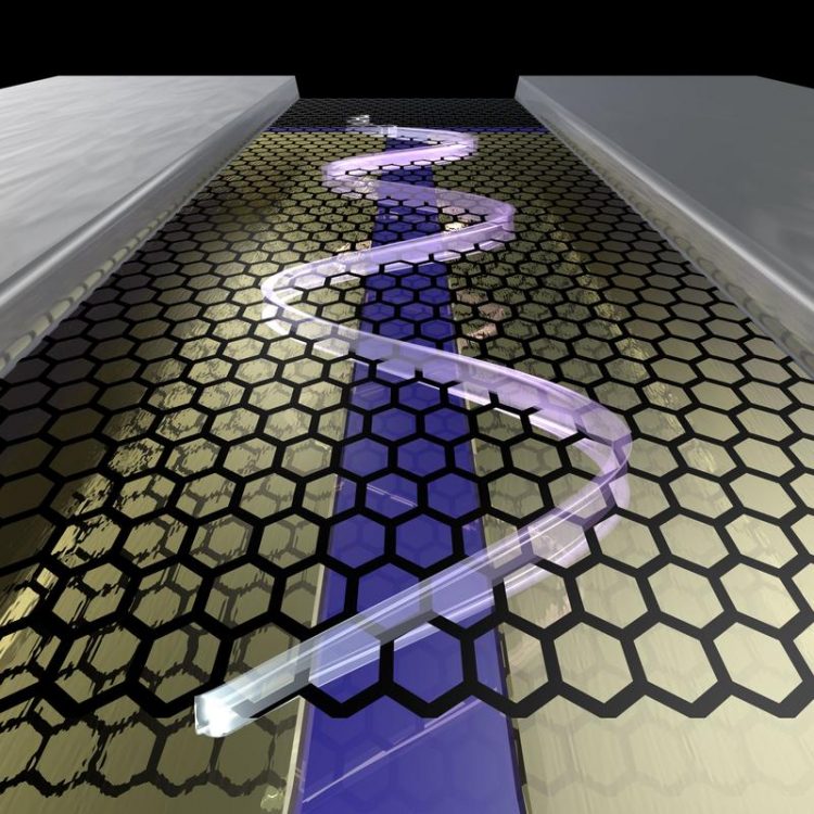
The honeycomb grid provides an atomic graphene layer stretched between 2 electrical contacts (silver). The lower area contains two control electrodes (gold), which are used to generate an electrical © Adapted with permission from Rickhaus et al., Nature Communications (2015).
For some years, the research group led by Professor Christian Schönenberger at the Swiss Nanoscience Institute and the Department of Physics has been looking at graphene, the “miracle material”.
Scientists at the University of Basel have developed methods that allow them to stretch, examine and manipulate layers of pure graphene. In doing so, they discovered that electrons can move in this pure graphene practically undisturbed – similar to rays of light. To lead the electrons from one specific place to another, they planned to actively guide the electrons along a predefined path in the material.
Electrical and magnetic fields combined
For the first time, the scientists in Basel have succeeded in switching the guidance of the electrons on and off and guiding them without any loss. The mechanism applied is based on a property that occurs only in graphene. Combining an electrical field and a magnetic field means that the electrons move along a snake state. The line bends to the right, then to the left. This switch is due to the sequence of positive and negative mass – a phenomenon that can only be realized in graphene and could be used as a novel switch.
“A nano-switch of this type in graphene can be incorporated into a wide variety of devices and operated simply by altering the magnetic field or the electrical field,” comments Professor Christian Schönenberger on the latest results from his group. Teams of physicists from Regensburg, Budapest and Grenoble were also involved in the study published in “Nature Communications”.
Material with special properties
Graphene is a very special material with promising properties. It is made up of a single layer of carbon atoms but is still very mechanically durable and resistant. Its excellent electrical conductivity in particular makes graphene the subject of research by numerous teams of scientists around the world.
The particular properties of this material were examined theoretically several decades ago. However, it was not until 2004 that physicists Andre Geim and Kostya Novoselov succeeded in producing graphene for experimental tests. The two researchers used scotch tape to peel away individual two-dimensional graphene layers from the original material, graphite. They received the 2010 Nobel Prize for Physics for this seemingly simple method, which enabled experimental graphene research for the first time. Since then, researchers worldwide have perfected the production process with tremendous speed.
Original source
Peter Rickhaus, Peter Makk, Ming-Hao Liu, Endre Tovari, Markus Weiss, Romain Maurand, Klaus Richter, and Christian Schönenberger
Snake trajectories in ultraclean graphene p–n junctions
Nature Communications 6:6470, published 3 March 2015, doi: 10.1038/ncomms7470
Further Information
Prof. Dr. Christian Schönenberger, University of Basel/Swiss Nanoscience Institute, phone: +41 61 267 36 90, email: christian.schoenenberger@unibas.ch
http://www.nature.com/ncomms/2015/150303/ncomms7470/full/ncomms7470.html – Abstract & Full Text
https://nanoelectronics.unibas.ch – Research group Prof. Dr. Christian Schönenberger
Media Contact
More Information:
http://www.unibas.chAll latest news from the category: Physics and Astronomy
This area deals with the fundamental laws and building blocks of nature and how they interact, the properties and the behavior of matter, and research into space and time and their structures.
innovations-report provides in-depth reports and articles on subjects such as astrophysics, laser technologies, nuclear, quantum, particle and solid-state physics, nanotechnologies, planetary research and findings (Mars, Venus) and developments related to the Hubble Telescope.


Newest articles

Silicon Carbide Innovation Alliance to drive industrial-scale semiconductor work
Known for its ability to withstand extreme environments and high voltages, silicon carbide (SiC) is a semiconducting material made up of silicon and carbon atoms arranged into crystals that is…

New SPECT/CT technique shows impressive biomarker identification
…offers increased access for prostate cancer patients. A novel SPECT/CT acquisition method can accurately detect radiopharmaceutical biodistribution in a convenient manner for prostate cancer patients, opening the door for more…

How 3D printers can give robots a soft touch
Soft skin coverings and touch sensors have emerged as a promising feature for robots that are both safer and more intuitive for human interaction, but they are expensive and difficult…

