Futuristic Components on Silicon Chips, Fabricated Successfully
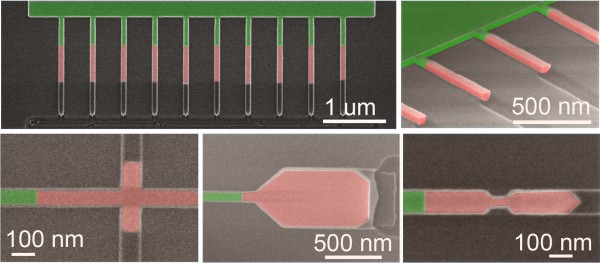
H. Schmid/IBM Scanning electron microscope images of single crystal structures fabricated using template-assisted selective epitaxy. For better visibility, the silicon is colored in green, and the compound semiconductor in red.
A team of IBM researchers in Zurich, Switzerland with support from colleagues in Yorktown Heights, New York has developed a relatively simple, robust and versatile process for growing crystals made from compound semiconductor materials that will allow them be integrated onto silicon wafers — an important step toward making future computer chips that will allow integrated circuits to continue shrinking in size and cost even as they increase in performance.
Appearing this week on the cover of the journal Applied Physics Letters, from AIP Publishing, the work may allow an extension to Moore's Law, the famous observation by Gordon Moore that the number of transistors on an integrated circuit double about every two years. In recent years some in the industry have speculated that our ability to keep pace with Moore's Law may become exhausted eventually unless new technologies come along that will lend it leash.
“The whole semiconductor industry wants to keep Moore’s Law going. We need better performing transistors as we continue down-scaling, and transistors based on silicon won’t give us improvements anymore,” said Heinz Schmid, a researcher with IBM Research GmbH at Zurich Research Laboratory in Switzerland and the lead author on the paper.
For consumers, extending Moore's Law will mean continuing the trend of new computer devices having increasing speed and bandwidth at reduced power consumption and cost. The new technique may also impact photonics on silicon, with active photonic components integrated seamlessly with electronics for greater functionality.
How the Work was Done
The IBM team fabricated single crystal nanostructures, such as nanowires, nanostructures containing constrictions, and cross junctions, as well as 3-D stacked nanowires, made with so-called III–V materials. Made from alloys of indium, gallium and arsenide, III-V semiconductors are seen as a possible future material for computer chips, but only if they can be successfully integrated onto silicon. So far efforts at integration have not been very successful.
The new crystals were grown using an approach called template-assisted selective epitaxy (TASE) using metal organic chemical vapor deposition, which basically starts from a small area and evolves into a much larger, defect-free crystal. This approach allowed them to lithographically define oxide templates and fill them via epitaxy, in the end making nanowires, cross junctions, nanostructures containing constrictions and 3-D stacked nanowires using the already established scaled processes of Si technology.
“What sets this work apart from other methods is that the compound semiconductor does not contain detrimental defects, and that the process is fully compatible with current chip fabrication technology,” said Schmid. “Importantly the method is also economically viable.”
He added that more development will be required to achieve the same control over performance in III-V devices as currently exists for silicon. But the new method is the key to actually integrating the stacked materials on the silicon platform, Schmid said.
The article, “Template-assisted selective epitaxy of III–V nanoscale devices for co-planar heterogeneous integration with Si,” is authored by H. Schmid, M. Borg, K. Moselund, L. Gignac, C. M. Breslin, J. Bruley, D. Cutaia and H. Riel. It will be published in the journal Applied Physics Letters on June 8, 2015 (DOI: 10.1063/1.4921962). After that date, it can be accessed at: http://scitation.aip.org/content/aip/journal/apl/106/23/10.1063/1.4921962
ABOUT THE JOURNAL
Applied Physics Letters features concise, rapid reports on significant new findings in applied physics. The journal covers new experimental and theoretical research on applications of physics phenomena related to all branches of science, engineering, and modern technology. See: http://apl.aip.org
Contact Information
Jason Socrates Bardi
+1 240-535-4954
jbardi@aip.org
@jasonbardi
Media Contact
All latest news from the category: Physics and Astronomy
This area deals with the fundamental laws and building blocks of nature and how they interact, the properties and the behavior of matter, and research into space and time and their structures.
innovations-report provides in-depth reports and articles on subjects such as astrophysics, laser technologies, nuclear, quantum, particle and solid-state physics, nanotechnologies, planetary research and findings (Mars, Venus) and developments related to the Hubble Telescope.


Newest articles
Combatting disruptive ‘noise’ in quantum communication
In a significant milestone for quantum communication technology, an experiment has demonstrated how networks can be leveraged to combat disruptive ‘noise’ in quantum communications. The international effort led by researchers…
Stretchable quantum dot display
Intrinsically stretchable quantum dot-based light-emitting diodes achieved record-breaking performance. A team of South Korean scientists led by Professor KIM Dae-Hyeong of the Center for Nanoparticle Research within the Institute for…
Internet can achieve quantum speed with light saved as sound
Researchers at the University of Copenhagen’s Niels Bohr Institute have developed a new way to create quantum memory: A small drum can store data sent with light in its sonic…

