Curved nanochannels allow independent tuning of charge and spin currents
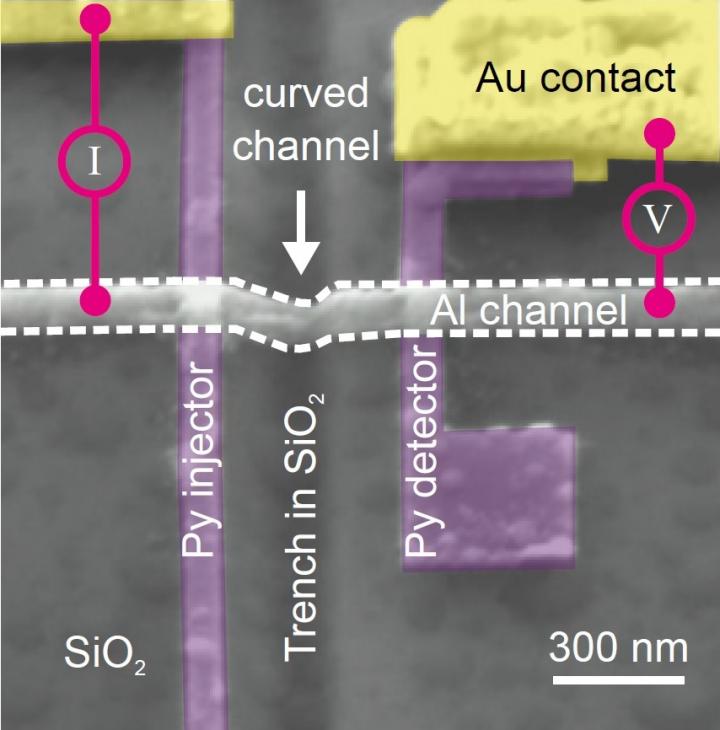
Scanning electron microscope image of a non-local spin-valve with a curved nano-channel as used in this study. Transport of pure spin current has been achieved and can be controlled by changing the 3D geometry of the nano-channel. Credit: Das et al, Nano Letters
Das started with two main questions: how to tune spin current using geometry, and how to create spin transport in a 3D nanostructure. Electron spin is a quantum mechanical property, a magnetic moment that can be used to transfer or store information. Spin is already used in memory storage, and could also be used in logic circuits.
Curved architecture
'So far, most spintronic devices have been based on a flat structure. We wanted to find out how the spin currents behave in a curved channel', says Das. Using silicon oxide substrates with trenches created by an ion beam, designed at the HZDR in Dresden by Dr. Denys Makarov, Das grew aluminum nanochannels that crossed the trenches. In this curved architecture, the thickness of the aluminum varies at nanoscale dimensions, shorter than the spin relaxation length.
Das used different sized trenches and measured both spin resistance and charge currents. 'What we discovered is that variations in the trench size affect spin and charge transport in the channel differently', Das explains. 'We were therefore able to independently tune both spin and charge currents based on the channel geometry.'
Novel functionalities
His colleague Dr. Carmine Ortix from Utrecht University created a theoretical model describing this phenomenon. 'Our theory clearly demonstrates that it is possible to independently tune the spin and charge characteristics using the shape of the materials alone.
This possibility overcomes the existing technological hurdles for the applicability of spintronics in modern electronics', says Dr. Ortix. 'Extending low-dimensional structures into the three-dimensional space can provide the means to modify conventional functionalities or even launch completely novel functionalities by suitably tailoring the shape of real materials.'
'This discovery is important because it allows us to tune spintronic components to match both the spin current and the charge current of electronic circuits', says Das. 'It enables the efficient integration of spin injectors and detectors or spin transistors into modern 3D circuitry.' This could help to create more energy-efficient electronics, as spintronics is an attractive way of creating low-power devices. 'And we can now use our model to purpose-design channels.'
###
EU project
The study was performed as part of the FET European project 'Curved nanomembranes for Topological Quantum Computation'. The experiments were initiated and supervised by Dr. Ivan Vera-Marun at the University of Manchester. Dr. Kumar Sourav Das performed the experiments as a part of his Ph.D. project in the Physics of Nanodevices group led by Prof. Bart van Wees. This group is part of the Zernike Institute for Advanced Materials at the University of Groningen. The theoretical model was created by Dr. Carmine Ortix at Utrecht University and colleagues from Italy.
Reference: Kumar Sourav Das, Denys Makarov. Paola Gentile. Mario Cuoco, Bart J. van Wees, Carmine Ortix and Ivan J. Vera-Marun: Independent Geometrical Control of Spin and Charge Resistances in Curved Spintronics. Nano Letters 13 September 20119
Media Contact
All latest news from the category: Physics and Astronomy
This area deals with the fundamental laws and building blocks of nature and how they interact, the properties and the behavior of matter, and research into space and time and their structures.
innovations-report provides in-depth reports and articles on subjects such as astrophysics, laser technologies, nuclear, quantum, particle and solid-state physics, nanotechnologies, planetary research and findings (Mars, Venus) and developments related to the Hubble Telescope.


Newest articles

Silicon Carbide Innovation Alliance to drive industrial-scale semiconductor work
Known for its ability to withstand extreme environments and high voltages, silicon carbide (SiC) is a semiconducting material made up of silicon and carbon atoms arranged into crystals that is…

New SPECT/CT technique shows impressive biomarker identification
…offers increased access for prostate cancer patients. A novel SPECT/CT acquisition method can accurately detect radiopharmaceutical biodistribution in a convenient manner for prostate cancer patients, opening the door for more…

How 3D printers can give robots a soft touch
Soft skin coverings and touch sensors have emerged as a promising feature for robots that are both safer and more intuitive for human interaction, but they are expensive and difficult…

