Combined effort for structural determination
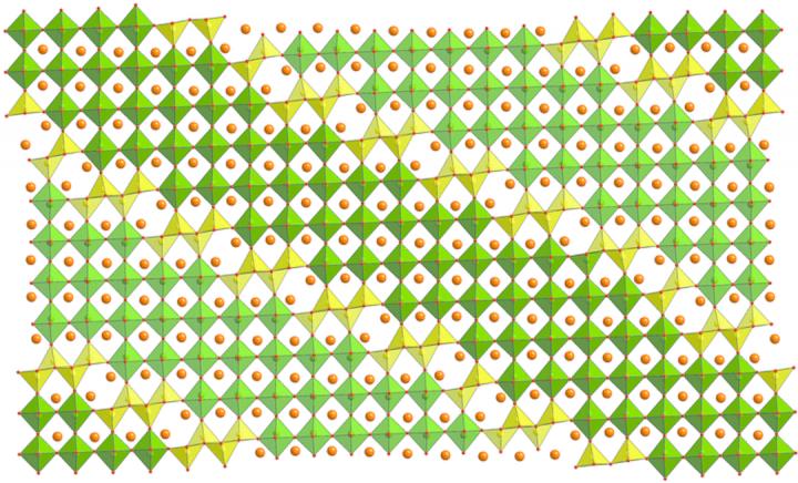
This is the refined structure of (Pb,Bi)1 - xFe1 + xO3 - y. Credit: Batuk et al.
Electron crystallography has begun to be used routinely for solving otherwise intractable structures. When performed in an aberration-corrected microscope and combined with spectroscopic techniques, it can offer unprecedented detail down to sub-angstrom resolution.
“The result of all this progress is that electron crystallography gives answers to more and more questions that used to be the domain of X-ray or neutron diffraction, and is especially useful when the X-ray or neutron experiment needs to be performed on a powder material, which limits the diffraction information available,” explains Lukas Palatinus of the Czech Academy of Sciences in Prague in a commentary piece in Acta Crystallographica Section B [Palatinus (2015). Acta Cryst. B71, 125-126; doi: 10.1107/S2052520615005910].
Palatinus points out that when confronted with modulated structures, in which every atomic position is perturbed from one unit cell to the next by a modulation function, the construction of the structure model is much more complicated than for non-modulated materials.
While effective techniques have been developed techniques to solve this problem from single crystal diffraction data, for powder diffraction data another approach to get around the problem is needed, which is where the work of Batuk and colleagues comes to the fore.
Batuk and colleagues have now shown how electron crystallography tools can be used to sidestep the limitations of powder diffraction and complement the structure analysis of modulated structures by powder diffraction. “The authors combine the results of their previous research with new results to provide an impressive overview of the available methods and information they can provide,” explains Palatinus.
The team investigated a series of anion-deficient perovskites to demonstrate proof of principle. In these materials, modulation arises as a consequence of the presence of crystallographic shear planes that have an average periodicity that is not in synchrony with the materials' basic periodicity.
Palatinus also points out that the choice of these materials was good for the given purpose. “These structures exhibit a wide variety of features that complicate the structure analysis of modulated structures from powder patterns,” explains Palatinus. “It allowed the authors to illustrate many techniques and applications like the simultaneous imaging of heavy and light elements, atomic resolution chemical mapping or the mapping of the coordination number.”
Additionally, given the advent of perovskites in recent years as the focus of research into solar panel materials and other semiconductor applications new detailed information about their structures and properties are increasingly important.
“The local crystallographic information acquired using the scanning transmission electron microscopy (STEM)-based methods in combination with the refinement from powder diffraction data can significantly improve the reliability of the crystal structure investigation,” Batuk and colleagues report.
Of course, electron crystallography is very unlikely to make X-ray or neutron diffraction redundant any time soon, points out Palatinus, not least because a lot of materials are too short lived under the degrading eye of the electron beam. Moreover, electron techniques generally cannot be applied in situ in chemical reaction environments nor under pressure, instead requiring near vacuum conditions.
Nevertheless, he adds that the team “shows convincingly how the electron crystallography methods have grown to a rich source of detailed information on the crystal structures, and it should convince any reader that resorting to these methods may very quickly solve problems that seem intractable by the more traditional approaches.”
It seems that as with many areas of study, a combined effort, the teamwork between different techniques that can complement each others, is needed to obtain the best results. “The key to success indeed lies in exploiting the complementarity and synergy between various methods,” Palatinus says.
Media Contact
All latest news from the category: Physics and Astronomy
This area deals with the fundamental laws and building blocks of nature and how they interact, the properties and the behavior of matter, and research into space and time and their structures.
innovations-report provides in-depth reports and articles on subjects such as astrophysics, laser technologies, nuclear, quantum, particle and solid-state physics, nanotechnologies, planetary research and findings (Mars, Venus) and developments related to the Hubble Telescope.


Newest articles

Silicon Carbide Innovation Alliance to drive industrial-scale semiconductor work
Known for its ability to withstand extreme environments and high voltages, silicon carbide (SiC) is a semiconducting material made up of silicon and carbon atoms arranged into crystals that is…

New SPECT/CT technique shows impressive biomarker identification
…offers increased access for prostate cancer patients. A novel SPECT/CT acquisition method can accurately detect radiopharmaceutical biodistribution in a convenient manner for prostate cancer patients, opening the door for more…

How 3D printers can give robots a soft touch
Soft skin coverings and touch sensors have emerged as a promising feature for robots that are both safer and more intuitive for human interaction, but they are expensive and difficult…

