Can Perovskites and Silicon Team Up to Boost Industrial Solar Cell Efficiencies?
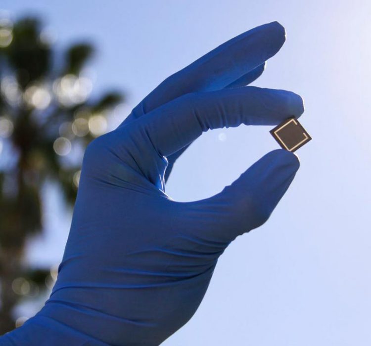
Rongrong Cheacharoen/Stanford University 1 cm2 monolithic perovskite-silicon tandem solar cell.
Silicon solar cells dominate 90 percent of the global photovoltaic market today, yet the record power conversion efficiency of silicon photovoltaics has progressed merely from 25 percent to 25.6 percent during the past 15 years — meaning the industry is keen to explore alternatives.
A collaboration between the Massachusetts Institute of Technology (MIT) and Stanford University may be poised to shake things up in the solar energy world. By exploring ways to create solar cells using low-cost manufacturing methods, the team has developed a novel prototype device that combines perovskite with traditional silicon solar cells into a two-terminal “tandem” device.
As the team reports in the journal Applied Physics Letters, from AIP Publishing, their new tandem cells have the potential to achieve significantly higher energy conversion efficiencies than standard single-junction silicon solar cells.
Perovskite is an inexpensive crystalline material that can easily be produced in labs and, as it turns out, stacking it atop a conventional silicon solar cell forms a tandem that has the potential to improve the cell’s overall efficiency, a measure of the amount of sunlight the cell can convert into electricity.
The team focused on tandem solar cells because there was big room for improvement in their cost and market penetration. Tandem solar cells have only garnered a worldwide market share of 0.25 percent compared to silicon solar cells’ 90 percent. “Despite having higher efficiency, tandems are traditionally made using expensive processes — making it difficult for them to compete economically,” said Colin Bailie, a Ph.D. student at Stanford and an author on the new paper.
Designing low-cost perovskite-silicon tandem solar cells
The team’s tandem approach focuses on keeping costs low and “integrates perovskite solar cells monolithically — building them sequentially in layers — onto a silicon solar cell, without significant optical or electrical losses, by using commonly available semiconductor materials and deposition methods,” explained Jonathan P. Mailoa, a graduate student in MIT’s Photovoltaic Research Laboratory and another co-author on the paper.
Before creating the tandems, the researchers first needed to design an interlayer to facilitate electronic charge carrier recombination without significant energy losses. “Fortunately, the physical concepts already exist for other types of multijunction solar cells, so we simply needed to find the best interlayer material combination for the perovskite-silicon pair,” Mailoa said.
To form a connecting layer, known technically as the semiconductor “tunnel junction,” between the two sub-cells, the team used degenerately doped p-type and n-type silicon, which facilitates the recombination of positive charge carriers (holes) from the silicon solar cell and negative charge carriers (electrons) from the perovskite solar cell.
Because the two silicon layers are highly doped, “the energy barrier between them is thin enough so that electrons and holes in the semiconductor easily pass through using quantum mechanical tunneling,” Mailoa added.
While electrons from a perovskite solar cell won’t normally enter this tunnel junction layer, a titanium-dioxide (TiO2) layer commonly used in perovskite solar cells works as an electron-selective contact for silicon. This allows electrons to flow from the perovskite solar cell through the TiO2 layer, eventually passing into the silicon tunnel junction, where they recombine with the holes from the silicon solar cell.
How do perovskite-silicon tandem solar cells work?
Once the tandem is set up, it relies on its multiple absorber layers to absorb different portions of the solar spectrum. “The perovskite absorbs all of the visible photons [higher in energy], for example, while the silicon absorbs the infrared photons [lower in energy],” Bailie said.
Splitting the solar spectrum allows these specialized absorbing layers to convert their range of the spectrum into electrical power much more efficiently than a single absorber can convert the entire solar spectrum on its own.
“This minimizes an undesirable process in solar cells called “thermalization,” in which the energy of an absorbed photon is released as heat until it reaches the energy of the absorber’s bandgap,” Bailie explained. “Using a high-bandgap absorber on top of the low-bandgap absorber recovers some of this energy in the high-energy photons that would otherwise be ‘thermalized’ if absorbed in the low-bandgap absorber.”
Another key part of the tandem’s design is that it uses a serial connection, which means that the two solar cells are connected in a manner so that the same amount of current passes through each of the solar cells. In other words, the same amount of light is absorbed in each solar cell and their voltage is added together.
Efficiency evolution ahead
The team’s tandem “demonstrated an open-circuit voltage of 1.65 V, which is essentially the sum of top and bottom cells, with very little voltage loss,” said Tonio Buonassisi, an associate professor of mechanical engineering at MIT who led the research.
An open-circuit voltage of 1.65 V was the highest best-case scenario the team had predicted, which indicates that their tunnel junction performs very well.
But an efficiency evolution is on the horizon. The efficiency record for single-junction perovskite cells ranges from 16 to 20 percent, depending on the formula used. “By contrast, the perovskite in our tandem is based on a technology that achieves only 13 percent in our lab as a single-junction device,” said Bailie. “Improving the quality of our perovskite layer will lead to better tandem devices.”
Another area for improving the tandem’s efficiency is by “reducing parasitic optical losses in other layers of the multijunction solar cell devices and predicting their efficiency potentials through simulation to determine whether or not this approach is truly cost effective,” added Mailoa.
The team also plans “to make improvements to the silicon bottom cell,” said Buonassisi. “The back contact isn’t well passivated, so we lose power at longer wavelengths. But the photovoltaic industry has developed several solutions for this problem…we just need to incorporate one best practice into our next-generation devices.”
While their work is still far from becoming commercially available, it frees other researchers to start to focus their efforts on important aspects of the multijunction device to help further improve both its stability and efficiencies in the future.
“This is the first step in the evolution of a technology that has the potential to disrupt the photovoltaic industry,” noted Bailie.
The article, “A 2-terminal perovskite/silicon multijunction solar cell enabled by a silicon tunnel junction,” is authored by Jonathan P. Mailoa, Colin D. Bailie, Eric C. Johlin, Eric T. Hoke, Austin J. Akey, William H. Nguyen, Michael D. McGehee and Tonio Buonassisi. It will be published in the journal Applied Physics Letters on March 24, 2015 (DOI: 10.1063/1.4914179). After that date, it can be accessed at: http://scitation.aip.org/content/aip/journal/apl/106/12/10.1063/1.4914179
The authors of this paper are affiliated with the Massachusetts Institute of Technology and Stanford University.
This work was supported by the U.S. Department of Energy (DOE) under Contract No. DE-EE0006707, and by the Bay Area Photovoltaic Consortium (BAPVC) under Contract No. DE-EE0004946.
ABOUT THE JOURNAL
Applied Physics Letters features concise, rapid reports on significant new findings in applied physics. The journal covers new experimental and theoretical research on applications of physics phenomena related to all branches of science, engineering, and modern technology. See: http://apl.aip.org
Contact Information
Jason Socrates Bardi
American Institute of Physics
jbardi@aip.org
240-535-4954
@jasonbardi
Media Contact
All latest news from the category: Physics and Astronomy
This area deals with the fundamental laws and building blocks of nature and how they interact, the properties and the behavior of matter, and research into space and time and their structures.
innovations-report provides in-depth reports and articles on subjects such as astrophysics, laser technologies, nuclear, quantum, particle and solid-state physics, nanotechnologies, planetary research and findings (Mars, Venus) and developments related to the Hubble Telescope.


Newest articles

Properties of new materials for microchips
… can now be measured well. Reseachers of Delft University of Technology demonstrated measuring performance properties of ultrathin silicon membranes. Making ever smaller and more powerful chips requires new ultrathin…

Floating solar’s potential
… to support sustainable development by addressing climate, water, and energy goals holistically. A new study published this week in Nature Energy raises the potential for floating solar photovoltaics (FPV)…

Skyrmions move at record speeds
… a step towards the computing of the future. An international research team led by scientists from the CNRS1 has discovered that the magnetic nanobubbles2 known as skyrmions can be…

