A new spin on electronics
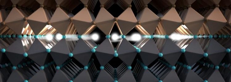
The spin of electrons transports information in this conducting layer between two isolators Image: Christoph Hohmann / NIM
Modern computer technology is based on the transport of electric charge in semiconductors. But this technology’s potential will be reaching its limits in the near future, since the components deployed cannot be miniaturized further. But, there is another option: using an electron’s spin, instead of its charge, to transmit information. A team of scientists from Munich and Kyoto is now demonstrating how this works.
Computers and mobile devices continue providing ever more functionality. The basis for this surge in performance has been progressively extended miniaturization. However, there are fundamental limits to the degree of miniaturization possible, meaning that arbitrary size reductions will not be possible with semiconductor technology.
Researchers around the world are thus working on alternatives. A particularly promising approach involves so-called spin electronics. This takes advantage of the fact that electrons possess, in addition to charge, angular momentum – the spin. The experts hope to use this property to increase the information density and at the same time the functionality of future electronics.
Together with colleagues at the Kyoto University in Japan scientists at the Walther-Meißner-Institute (WMI) and the Technical University of Munich (TUM) in Garching have now demonstrated the transport of spin information at room temperature in a remarkable material system.
A unique boundary layer
In their experiment, they demonstrated the production, transport and detection of electronic spins in the boundary layer between the materials lanthanum-aluminate (LaAlO2) and strontium-titanate (SrTiO3). What makes this material system unique is that an extremely thin, electrically conducting layer forms at the interface between the two non-conducting materials: a so-called two-dimensional electron gas.
The German-Japanese team has now shown that this two-dimensional electron gas transports not only charge, but also spin. “To achieve this we first had to surmount several technical hurdles,” says Dr Hans Hübl, scientist at the Chair for Technical Physics at TUM and Deputy Director of the Walther-Meißner-Institute. “The two key questions were: How can spin be transferred to the two-dimensional electron gas and how can the transport be proven?”
Information transport via spin
The scientists solved the problem of spin transfer using a magnetic contact. Microwave radiation forces its electrons into a precession movement, analogous to the wobbling motion of a top. Just as in a top, this motion does not last forever, but rather, weakens in time – in this case by imparting its spin onto the two-dimensional electron gas.
The electron gas then transports the spin information to a non-magnetic contact located one micrometer next to the contact. The non-magnetic contact detects the spin transport by absorbing the spin, building up an electric potential in the process. Measuring this potential allowed the researchers to systematically investigate the transport of spin and demonstrate the feasibility of bridging distances up to one hundred times larger than the distance of today’s transistors.
Based on these results, the team of scientists is now researching to what extent spin electronic components with novel functionality can be implemented using this system of materials.
The research was funded by the German Research Foundation (DFG) in the context of the Cluster of Excellence “Nanosystems Initiative Munich” (NIM).
Publication:
Strong evidence for d-electron spin transport at room temperature at a LaAlO3/SrTiO3 interface. R. Ohshima, Y. Ando, K. Matsuzaki, T. Susaki, M. Weiler, S. Klingler, H. Huebl, E. Shikoh, T. Shinjo, S.T.B Goennenwein and M. Shiraishi. Nature Materials, Advanced Online Publication 13. Februar 2017. DOI:10.1038/nmat4857
http://www.nature.com/nmat/journal/vaop/ncurrent/full/nmat4857.html
Contact:
Dr. Hans Gregor Hübl
Magnetism, Spintronics and Nano Electromechanics
Deputy Director of Walther-Meißner-Institute, Bavarian Academy of Science,
Chair for Technical Physics (E23) at Technical University of Munich
Walther-Meißner-Straße 8, 85748 Garching, Germany
Tel.: +49 89 289 14204 – E-Mail: hans.huebl@tum.de – Web: http://www.wmi.badw.de
Media Contact
All latest news from the category: Physics and Astronomy
This area deals with the fundamental laws and building blocks of nature and how they interact, the properties and the behavior of matter, and research into space and time and their structures.
innovations-report provides in-depth reports and articles on subjects such as astrophysics, laser technologies, nuclear, quantum, particle and solid-state physics, nanotechnologies, planetary research and findings (Mars, Venus) and developments related to the Hubble Telescope.


Newest articles
Solving the riddle of the sphingolipids in coronary artery disease
Weill Cornell Medicine investigators have uncovered a way to unleash in blood vessels the protective effects of a type of fat-related molecule known as a sphingolipid, suggesting a promising new…
Rocks with the oldest evidence yet of Earth’s magnetic field
The 3.7 billion-year-old rocks may extend the magnetic field’s age by 200 million years. Geologists at MIT and Oxford University have uncovered ancient rocks in Greenland that bear the oldest…
Decisive breakthrough for battery production
Storing and utilising energy with innovative sulphur-based cathodes. HU research team develops foundations for sustainable battery technology Electric vehicles and portable electronic devices such as laptops and mobile phones are…

