Building Electronics From the Ground Up
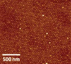
Chemical Communications<br>Nanodots of iron oxide were laid out in a highly ordered pattern without the use of templates. The average diameter of the particles was 25 nanometers, with regular spacing of 45 nm.
But our expectation that the next shopping season will inevitably offer an upgrade to more-powerful gadgets largely depends on size – namely, the ability of the industry to shrink transistors so that more can fit on ever-tinier chip surfaces.
Engineers have been up to the task of electronics miniaturization for decades now, and the principle that the computer industry will be able to do it on a regular schedule – as codified in Moore’s Law – won’t come into doubt any time soon, thanks to researchers like the University of South Carolina’s Chuanbing Tang.
Tang is a leader in constructing miniscule structures from the bottom up, rather than the top down. Currently, modern electronics are primarily fabricated by the latter method: the smooth surface of a starting material – say, a wafer of silicon – is etched through micro- or nanolithography to establish a pattern on it. The top-down method might involve a prefabricated template, such as a photomask, to establish the pattern. But the approach is becoming more and more challenging, because reducing the size of the features on the requisite templates is getting extremely expensive as engineers work their way further down the nanoscale. “Going from 500 to sub-30 nanometers is cost prohibitive for large-scale production,” said Tang, an assistant professor in the department of chemistry and biochemistry in USC’s College of Arts and Sciences.
As a chemist, Tang uses a bottom-up approach: he works with the individual molecules that go onto a surface, coaxing them to self-arrange into the patterns needed. One established method of doing this involves block copolymers, in which a polymer chain is made up of two or more sections of different polymerized monomers.
If the different block sections are properly designed, the blocks will self-aggregate when placed on a surface, and the aggregation can be harnessed to create desirable patterns on the nanoscale without the need for any templates. Di-block copolymers of poly(ethylene oxide) and polystyrene, for example, have been used to construct highly ordered arrays of perpendicular cylinders of nanoscale materials. Solvent evaporation, or annealing, of these polymers on surfaces exerts an external directional field that can enhance the patterning process and create nearly defect-free arrays.
Tang’s laboratory just published a paper for the special “Emerging Investigators 2013” issue of the journal Chemical Communications that takes this method to a new level. Working together with graduate student Christopher Hardy, Tang led a team that fabricated nanoparticles of pure, crystalline iron oxide with controlled size and spacing on silicon wafers by covalently incorporating a ferrocene moiety into a tri-block copolymer.
Incorporating metals into nanoscale designs is crucial for fabricating electronic devices, and Tang’s method is a step forward for the field. Because ferrocene is covalently bonded to the block copolymer, there is no need for a complexation step to add a metal-containing compound to the surface – a burdensome requirement of most previous methods. Moreover, their technique is a step beyond related polymer systems that contain covalent ferrocenylsilane linkages, in which removal of the organic components leaves behind silicon oxide as an impurity in the metal oxide.
The technique is a promising addition to the available tools for addressing the chronic need to decrease the size of electronic components. “The industry won’t replace top-down methods,” Tang said, “but they plan to use bottom-up together with the existing top-down methods soon.”
There’s versatility in the technique as well. “Here we use a ferrocene-containing polymer, which we convert into the inorganic iron oxide. But if we replace the ferrocene in the polymer with carbon precursor, we could make a perpendicular carbon nanorod, which would have a lot of potential uses,” Tang said. “Or we can incorporate a semi-conducting polymer, like polythiophene, which would be very useful in solar cell applications.”
The work was supported by Semiconductor Research Corporation (Task ID 2222.001) and National Science Foundation (CHE-1151479).
Media Contact
More Information:
http://www.sc.eduAll latest news from the category: Life Sciences and Chemistry
Articles and reports from the Life Sciences and chemistry area deal with applied and basic research into modern biology, chemistry and human medicine.
Valuable information can be found on a range of life sciences fields including bacteriology, biochemistry, bionics, bioinformatics, biophysics, biotechnology, genetics, geobotany, human biology, marine biology, microbiology, molecular biology, cellular biology, zoology, bioinorganic chemistry, microchemistry and environmental chemistry.


Newest articles

Properties of new materials for microchips
… can now be measured well. Reseachers of Delft University of Technology demonstrated measuring performance properties of ultrathin silicon membranes. Making ever smaller and more powerful chips requires new ultrathin…

Floating solar’s potential
… to support sustainable development by addressing climate, water, and energy goals holistically. A new study published this week in Nature Energy raises the potential for floating solar photovoltaics (FPV)…

Skyrmions move at record speeds
… a step towards the computing of the future. An international research team led by scientists from the CNRS1 has discovered that the magnetic nanobubbles2 known as skyrmions can be…

