Small modulator for big data
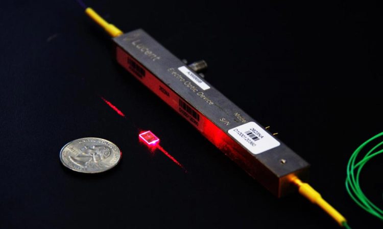
Conventional lithium niobate modulators [right] are the backbone of modern telecommunications, converting electronic data to optical information in fiber optic cables but are bulky, expensive and power hungry. This integrated, on-chip modulator [center] is 100 times smaller and 20 times more efficient. Credit: Harvard SEAS
Conventional lithium niobite modulators, the longtime workhorse of the optoelectronic industry, may soon go the way of the vacuum tube and floppy disc. Researchers from the Harvard John A. Paulson School of Engineering and Applied Sciences have developed a new method to fabricate and design integrated, on-chip modulators 100 times smaller and 20 times more efficient than current lithium niobite (LN) modulators.
The research is described in Nature.
“This research demonstrates a fundamental technological breakthrough in integrated photonics,” said Marko Loncar, the Tiantsai Lin Professor of Electrical Engineering at SEAS and senior author of the paper. “Our platform could lead to large-scale, very fast and ultra-low-loss photonic circuits, enabling a wide range of applications for future quantum and classical photonic communication and computation.”
Harvard's Office of Technology Development (OTD) has worked closely with the Loncar Lab on the formation of a startup company, HyperLight, that intends to commercialize a portfolio of foundational intellectual property related to this research. Readying the technology toward the launch of HyperLight has been aided by funding from OTD's Physical Sciences & Engineering Accelerator, which provides translational funding for research projects that show potential for significant commercial impact.
Lithium niobate modulators are the backbone of modern telecommunications, converting electronic data to optical information in fiber optic cables. However, conventional LN modulators are bulky, expensive and power hungry. These modulators require a drive voltage of 3 to 5 volts, significantly higher than that provided by typical CMOS circuitry, which provides about 1 volt. As a result, separate, power-consuming amplifiers are needed to drive the modulators, severely limiting chip-scale optoelectronic integration.
“We show that by integrating lithium niobate on a small chip, the drive voltage can be reduced to a CMOS-compatible level,” said Cheng Wang, co-first author of the paper, former PhD student and postdoctoral fellow at SEAS, and currently Assistant Professor at City University of Hong Kong. “Remarkably, these tiny modulators can also support data transmission rates up to 210 Gbit/s. It's like Antman – smaller, faster and better.”
“Highly-integrated yet high-performance optical modulators are very important for the closer integration of optics and digital electronics, paving the way towards future fiber-in-fiber-out opto-electronic processing engines,” said Peter Winzer, Director of Optical Transmission Research at Nokia Bell Labs, the industrial partner in this project, and coauthor of the paper. “We see this new modulator technology as a promising candidate for such solutions.”
Lithium niobite is considered by many in the field to be difficult to work with on small scales, an obstacle that has so far ruled out practical integrated, on-chip applications. In previous research, Loncar and his team demonstrated a technique to fabricate high-performance lithium niobate microstructures using standard plasma etching to physically sculpt microresonators in thin lithium niobate films.
Combining that technique with specially designed electrical components, the researchers can now design and fabricate an integrated, high-performance on-chip modulator.
“Previously, if you wanted to make modulators smaller and more integrated, you had to compromise their performance,” said Mian Zhang, a postdoctoral fellow at SEAS and co-first author of the research. “For example, existing integrated modulators can easily lose majority of the light as it propagates on the chip. In contrast, we have reduced losses by more than an order of magnitude. Essentially, we can control light without losing it.”
“Because a modulator is such a fundamental component of communication technology — with a role equivalent to that of a transistor in computation technology — the applications are enormous,” said Zhang. “The fact that these modulators can be integrated with other components on the same platform could provide practical solutions for next-generation long distance optical networks, data center optical interconnects, wireless communications, radar, sensing and so on.”
###
This research was co-authored by Xi Chen, Maxime Bertrand, Amirhassan Shams-Ansari, and Sethumadhavan Chandrasekhar.
It was supported in part by National Science Foundation and the Harvard University Office of Technology Development's Physical Sciences and Engineering Accelerator Award. Device fabrication was performed at the Harvard University Center for Nanoscale Systems (CNS), a member of the National Nanotechnology Coordinated Infrastructure Network (NNCI), which is supported by the National Science Foundation.
Media Contact
All latest news from the category: Information Technology
Here you can find a summary of innovations in the fields of information and data processing and up-to-date developments on IT equipment and hardware.
This area covers topics such as IT services, IT architectures, IT management and telecommunications.


Newest articles

Security vulnerability in browser interface
… allows computer access via graphics card. Researchers at Graz University of Technology were successful with three different side-channel attacks on graphics cards via the WebGPU browser interface. The attacks…

A closer look at mechanochemistry
Ferdi Schüth and his team at the Max Planck Institut für Kohlenforschung in Mülheim/Germany have been studying the phenomena of mechanochemistry for several years. But what actually happens at the…

Severe Vulnerabilities Discovered in Software to Protect Internet Routing
A research team from the National Research Center for Applied Cybersecurity ATHENE led by Prof. Dr. Haya Schulmann has uncovered 18 vulnerabilities in crucial software components of Resource Public Key…

