Testing miniature silicon chips

Many activities in our daily lives use products and devices based on silicon chips – from computers and televisions to medical equipment and defense systems. As these products and applications become increasingly complex and miniature, so must the chips.
Chips are manufactured on a silicon wafer. Each chip is surrounded by electrical contacts (‘plots’) through which data enters and exits. The plots are connected to each other through extremely fine wires. In 1994 the distance between the chip and plot was 200µm, and between plots 110µm; 10 years later these figures were reduced to 60µm and 45µm respectively.
During their manufacture, chips are tested at a number of stages. The final test evaluates the performance of the chip according to its end use. However this test proved problematic with the new generation of high density, fine pitch wafers – the existing needle-based technology was no longer viable as it did not allow the mass production of test cards.
Aware of the potential global market demand for such a technology and its importance for the European microelectronics industry André Belmont, former manager at SGS Thomson (now ST Microelectronics), founded French SME Mesatronic to address market demands.
Through EUREKA project E! 2277 NEWTECT, Mesatronic teamed up with Italian, French and Swiss partners to develop and patent D.O.D. Technology® (Die On Die) – a probe card technology based on a semiconductor process for testing the new generation of silicon wafers.
Now recognised as one of the best in the world, D.O.D. Technology® is the only probe card technology based on a semiconductor process. In addition to its ability to test the new generation of silicon wafers, a single card can test an average of one million wafers.
According to Belmont: “Our idea had great market potential, but we lacked funding and know-how. EUREKA, with its unique industry-oriented approach, gave us this opportunity.”
Partly thanks to EUREKA, Mesatronic has grown from a small European enterprise with two members of staff into a world leader in its field with 64 employees and an annual turnover of €9 million. Around €3 million of current turnover and 30 jobs are directly attributable to the NEWTECT project. With several world leaders as clients (including Motorola, Infineon, Philips and Texas Instruments), it is one of the only companies offering the whole range of tests for the new generation of wafers. Furthermore, since starting the project, Mesatronic has on two occasions secured private funding.
Mesatronic is also this year’s winner of the EUREKA Lynx Award for small to medium-sized high-tech enterprises whose participation in a EUREKA project has resulted in significant commercial and financial growth.
Media Contact
More Information:
http://www.eureka.be/success-storiesAll latest news from the category: Information Technology
Here you can find a summary of innovations in the fields of information and data processing and up-to-date developments on IT equipment and hardware.
This area covers topics such as IT services, IT architectures, IT management and telecommunications.
Newest articles
Superradiant atoms could push the boundaries of how precisely time can be measured
Superradiant atoms can help us measure time more precisely than ever. In a new study, researchers from the University of Copenhagen present a new method for measuring the time interval,…
Ion thermoelectric conversion devices for near room temperature
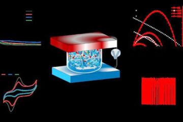
The electrode sheet of the thermoelectric device consists of ionic hydrogel, which is sandwiched between the electrodes to form, and the Prussian blue on the electrode undergoes a redox reaction…
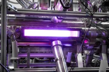
Zap Energy achieves 37-million-degree temperatures in a compact device
New publication reports record electron temperatures for a small-scale, sheared-flow-stabilized Z-pinch fusion device. In the nine decades since humans first produced fusion reactions, only a few fusion technologies have demonstrated…


