Breaking Into The Third Dimension Of Computer Chip Design

Despite continuous technical advances in the semiconductor industry, microchips are still composed of laterally-arranged (side-by-side) transistors on a silicon substrate. EUREKA project E! 2259 VSI developed new ways to break through this two dimensional approach and the restrictions it imposes by designing 3-D chips or Vertical System Integration (VSI).
This technology has immediate security benefits which are very desirable since chip cards often contain secure information or monetary values and, therefore, are subject to attack by hackers. “With the new technology, the top sides of the chips are inside the 3-D stack and therefore not accessible to mechanical attacks, electrical probing or a lot of other physical attacks,” says Wolfgang Gruber of Infineon Technologies AG, the German lead partner.
Infineon appreciates the co-operation a EUREKA project brings. “EUREKA helped us to find an equipment manufacturer with the necessary know how and skills that are only available in a few companies around the world,” explains Gruber. “The EUREKA label is a quality label most people associate with a sophisticated research project of high quality – a big advantage when it comes to convincing someone about your ideas!”
Increased flexibility
Using the 3-D chips, it is cheaper and easier to realise mixed technologies in a range of applications such as next-generation 3G mobile phones, smart cards and ’intelligent cars’.
The Austrian partner Datacon developed the machinery to construct the 3-D chips. “Through our close co-operation with Infineon we were able to produce a machine that could exceed the state-of-the-art in terms of production speed and accuracy,” says Christoph Scheiring, Manager of Advanced Technology at Datacon.
The partners have developed two versions of the 3-D stacking. The first will be ready for production in 2004, and is “a cost-efficient, two-layer technology called ’Solid Face to Face’ (F2F), in which one or more chips are attached and in contact with a base chip by a soldering process.” Gruber explains, “a demonstration chip card with a huge amount of memory capable of fulfilling requirements for future multi-application operating systems has been built.”
Work continues on the second version – a multi-layer technology based on F2F that will allow for wiring through a chip to the next chip, thus making stacks of three or more layers possible and further increasing the chip’s flexibility and security. This is due to be ready for production in 2007.
Media Contact
More Information:
http://www.eureka.be/success-storiesAll latest news from the category: Information Technology
Here you can find a summary of innovations in the fields of information and data processing and up-to-date developments on IT equipment and hardware.
This area covers topics such as IT services, IT architectures, IT management and telecommunications.
Newest articles
Superradiant atoms could push the boundaries of how precisely time can be measured
Superradiant atoms can help us measure time more precisely than ever. In a new study, researchers from the University of Copenhagen present a new method for measuring the time interval,…
Ion thermoelectric conversion devices for near room temperature
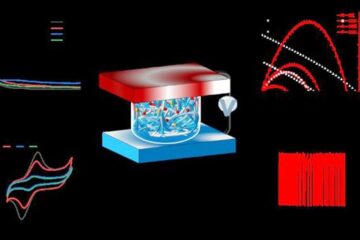
The electrode sheet of the thermoelectric device consists of ionic hydrogel, which is sandwiched between the electrodes to form, and the Prussian blue on the electrode undergoes a redox reaction…
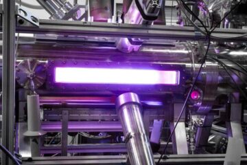
Zap Energy achieves 37-million-degree temperatures in a compact device
New publication reports record electron temperatures for a small-scale, sheared-flow-stabilized Z-pinch fusion device. In the nine decades since humans first produced fusion reactions, only a few fusion technologies have demonstrated…


