Micropatterning OLEDs using electron beam technology
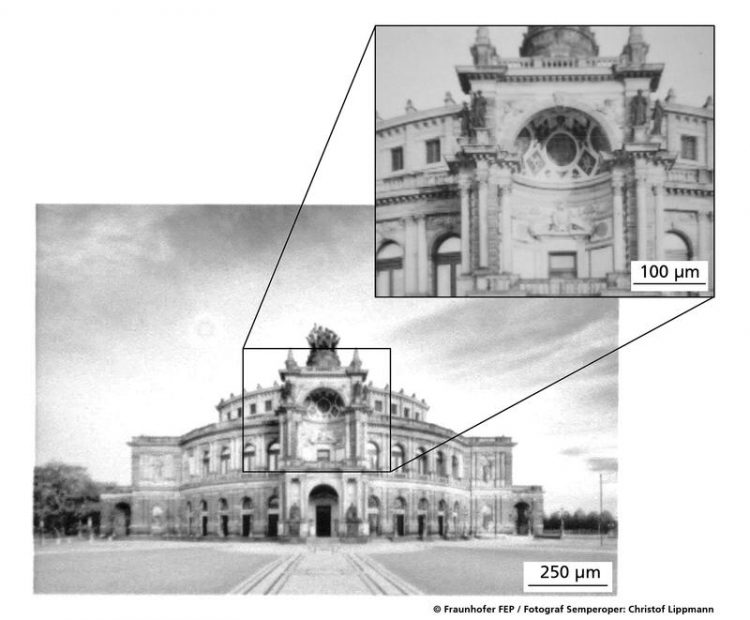
OLED patterned with an electron beam © Fraunhofer FEP / Photographer Semper Opera: Christof Lippmann
Fraunhofer FEP has years of experience in the field of processing organic semiconductor materials. Scientists here are also developing organic light-emitting diodes (OLEDs) and OLED microdisplays based on organic semiconductors.
Currently, techniques and new applications of electron beam technology – an additional area of core expertise at Fraunhofer FEP – are being particularly investigated in the field of organic electronics. Due to their outstanding optical and electronic properties, OLEDs have a broad range of potential applications in mobile electronics and displays.
Especially small displays with high pixel density, such as OLED microdisplays, are necessary for future applications such as augmented- or virtual-reality, for example. Researchers are now working on further miniaturizing while maintaining high resolution.
The patterning of the organic layers in OLEDs represents one of the biggest challenges, as conventional methods such as photolithography cannot be applied to organic semiconductor materials easily.
Fraunhofer FEP scientists have developed a novel approach to pattern the emission area of an OLED at high resolution. The patented technology uses an electron beam process, which takes place after finalizing the OLED including the encapsulation. Therefore it is possible to build the OLED highly productive and completely unpatterned, before the emission is individually modified by an adjusted electron beam process.
The energy of the electrons determines their penetration depth in the layer stack. With a suitable choice of process parameters, the encapsulation can also be penetrated by the electron beam and the luminous characteristics of the organic layers beneath will change without destroying or compromising the encapsulation itself. Depending on the application, it is even possible to modify individual layers directly.
“Continuous gray scales in an image can be created on a monochrome OLED using the electron beam, while at the same time the local current consumption is reduced. The longer the dwell time on one spot with the beam, the darker the OLED will appear there”, explains Elisabeth Bodenstein from the development team at Fraunhofer FEP. “An impressive example is the white OLED shown, in which the image of the famous Dresden Semperoper was structured with the electron beam in a hundred seconds.”
Even with a write time of less than two minutes, an impressive resolution of 12,700 dpi was attained – corresponding to 2 µm spacing of the image dots. The structuring of the OLED was carried out with an electron beam lithography system of Raith GmbH, the leading manufacturer of nanofabrication systems.
The process is highly adaptable – regardless of whether the OLED is applied to a rigid medium or flexible film, what color the OLED is, or whether the substrate is optically opaque, translucent, or transparent. The size of the substrate is universal as well and can be matched to the corresponding application. An enhancement to full-color patterning is being planned.
The Fraunhofer FEP scientists are now prepared to put this new technology into practice with industrial partners. The technology was developed within a project funded by the Fraunhofer Gesellschaft.
Fraunhofer FEP at the SID Display Week 2016
Talk
»OLED Microdisplays: Enabling Advanced Near-to-Eye Displays, Sensors, and Beyond«
Dr. Uwe Vogel, Session 52: OLED Displays II (Paper Number 52.2)
May 26, 2016, San Francisco Moscone Convention Center, Room 131
Exhibitor Forum
»Electron Beam Induced High-Resolution Modification of OLED Emission«
Elisabeth Bodenstein
Poster
»Electron Beam Induced High-Resolution Modification of OLED Emission«
Elisabeth Bodenstein, Poster number 208
May 26, 2016, San Francisco Moscone Convention Center, Room City View (Metreon)
Announcement
Fraunhofer FEP is pleased to be host of next SID ME 2017 Chapter Spring Meeting on March 13 – 14, 2017 in Dresden. First Call-for-Papers here:
www.fep.fraunhofer.de/sidme17
Press contact:
Annett Arnold
Fraunhofer Institute for Organic Electronics, Electron Beam and Plasma Technology FEP| Phone +49 351 2586 452 | Annett.Arnold@fep.fraunhofer.de
Winterbergstraße 28 | 01277 Dresden | Germany | www.fep.fraunhofer.de
Media Contact
All latest news from the category: Information Technology
Here you can find a summary of innovations in the fields of information and data processing and up-to-date developments on IT equipment and hardware.
This area covers topics such as IT services, IT architectures, IT management and telecommunications.


Newest articles
Bringing bio-inspired robots to life
Nebraska researcher Eric Markvicka gets NSF CAREER Award to pursue manufacture of novel materials for soft robotics and stretchable electronics. Engineers are increasingly eager to develop robots that mimic the…

Bella moths use poison to attract mates
Scientists are closer to finding out how. Pyrrolizidine alkaloids are as bitter and toxic as they are hard to pronounce. They’re produced by several different types of plants and are…
AI tool creates ‘synthetic’ images of cells
…for enhanced microscopy analysis. Observing individual cells through microscopes can reveal a range of important cell biological phenomena that frequently play a role in human diseases, but the process of…

