World's smallest optical implantable biodevice
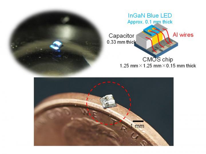
Size and design of the 1 mm3 optogenetic stimulator. Credit: Takashi Tokuda
For centuries, it has been known that chemicals can change neural behavior. The field of optogenetics proved that neural behavior can also be changed with mere light. It is now known that light can activate certain proteins in the brain to change brain patterns.
Accordingly, scientists have implanted optical devices to successfully control the behavior of rodents using nothing more than light of specific wavelengths as the stimulus. However, the devices are often bulky, akin to wearing a football helmet or something heavier, and cause discomfort and distress to the animals.
Takashi Tokuda, an associate professor at the Nara Institute of Science and Technology (NAIST), has been investigating ways to miniaturize implantable optical devices.
“Size is always the challenge. No one likes having large implants,” he says.
The miniaturization of implantable devices has been hindered by a dependency on electromagnetics. In such devices, both the voltage and the current decrease with a reduction in size, thus limiting the power. On the other hand, in devices that depend on photovoltaics, voltage remains unchanged as size is reduced.
The new device made by Tokuda's research team uses a complementary metal-oxide semiconductor that controls photovoltaic power. “We integrated two sets of photovoltaic cells onto semiconductor chips. Ten cells were integrated for powering, and seven cells for biasing,” he said.
The device includes an InGan LED chip, which causes the device to emit blue light. A more distinguishing feature of the device, however, is that it can be activated with infrared light. Infrared is used in many light therapies, because it can penetrate deep in the body, whereas blue light cannot go much deeper than the surface. Therefore, the device can be implanted several centimeters into the body.
At just 1 mm3 and 2.3 mg, the volume and weight of the device are almost one order of magnitude than any other reported device, leading Tokuda to call it “the world's smallest wireless optical neural stimulator.”
At the same time, Tokuda acknowledges that the device needs modifications before reaching its fullest potential.
“The device can be applied only for pulse stimulations and requires a charge time for each stimulation. Most optogenetics use multiple pulses. We need to improve the power receiving and conversion efficiency,” he said.
###
* This research has been supported by PRESTO (Precursory Research for Embryonic Science and Technology), one of the strategic basic research programs under Japan Science and Technology Agency.
Resource
Title: 1 mm3-sized Optical Neural Stimulator based on CMOS Integrated Photovoltaic Power Receiver
Authors: Takashi Tokuda*, Takaaki Ishizu, Wuthibenjaphonchai Nattakarn, Makito Haruta, Toshihiko Noda, Kiyotaka Sasagawa, Mohamad Sawan, and Jun Ohta
Publication: AIP Advances, 8, 045018
DOI: 10.1063/1.5024243
*Author for correspondence
Information about Prof. Ohta lab can be found at the following website: http://mswebs.
Media Contact
All latest news from the category: Power and Electrical Engineering
This topic covers issues related to energy generation, conversion, transportation and consumption and how the industry is addressing the challenge of energy efficiency in general.
innovations-report provides in-depth and informative reports and articles on subjects ranging from wind energy, fuel cell technology, solar energy, geothermal energy, petroleum, gas, nuclear engineering, alternative energy and energy efficiency to fusion, hydrogen and superconductor technologies.


Newest articles

Superradiant atoms could push the boundaries of how precisely time can be measured
Superradiant atoms can help us measure time more precisely than ever. In a new study, researchers from the University of Copenhagen present a new method for measuring the time interval,…

Ion thermoelectric conversion devices for near room temperature
The electrode sheet of the thermoelectric device consists of ionic hydrogel, which is sandwiched between the electrodes to form, and the Prussian blue on the electrode undergoes a redox reaction…

Zap Energy achieves 37-million-degree temperatures in a compact device
New publication reports record electron temperatures for a small-scale, sheared-flow-stabilized Z-pinch fusion device. In the nine decades since humans first produced fusion reactions, only a few fusion technologies have demonstrated…

