Two-Dimensional Semiconductor Comes Clean
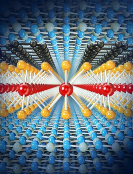
Gwan-Hyoung Lee/Yonsei University Schematic cross-section view of atomic layer of molybdenum disulfide contacted by graphene, and encapsulated between layers of insulating hexagonal boron nitride.
In work published this week in the Advance Online Publication on Nature Nanotechnology’s website, researchers at Columbia Engineering, Harvard, Cornell, University of Minnesota, Yonsei University in Korea, Danish Technical University, and the Japanese National Institute of Materials Science have shown that the performance of another 2D material—molybdenum disulfide (MoS2)—can be similarly improved by BN-encapsulation.
“These findings provide a demonstration of how to study all 2D materials,” says Hone, leader of this new study and director of Columbia’s NSF-funded Materials Research Science and Engineering Center. “Our combination of BN and graphene electrodes is like a ‘socket’ into which we can place many other materials and study them in an extremely clean environment to understand their true properties and potential. This holds great promise for a broad range of applications including high-performance electronics, detection and emission of light, and chemical/bio-sensing.”
Two-dimensional (2D) materials created by “peeling’” atomically thin layers from bulk crystals are extremely stretchable, optically transparent, and can be combined with each other and with conventional electronics in entirely new ways. But these materials—in which all atoms are at the surface—are by their nature extremely sensitive to their environment, and their performance often falls far short of theoretical limits due to contamination and trapped charges in surrounding insulating layers. The BN-encapsulated graphene that Hone’s group produced last year has 50× improved electronic mobility—an important measure of electronic performance—and lower disorder that enables the study of rich new phenomena at low temperature and high magnetic fields.
“We wanted to see what we could do with MoS2—it’s the best-studied 2D semiconductor, and, unlike graphene, it can form a transistor that can be switched fully ‘off’, a property crucial for digital circuits,” notes Gwan-Hyoung Lee, co-lead author on the paper and assistant professor of materials science at Yonsei. In the past, MoS2 devices made on common insulating substrates such as silicon dioxide have shown mobility that falls below theoretical predictions, varies from sample to sample, and remains low upon cooling to low temperatures, all indications of a disordered material. Researchers have not known whether the disorder was due to the substrate, as in the case of graphene, or due to imperfections in the material itself.
In the new work, Hone’s team created heterostructures, or layered stacks, of MoS2 encapsulated in BN, with small flakes of graphene overlapping the edge of the MoS2 to act as electrical contacts. They found that the room-temperature mobility was improved by a factor of about 2, approaching the intrinsic limit. Upon cooling to low temperature, the mobility increased dramatically, reaching values 5-50× that those measured previously (depending on the number of atomic layers). As a further sign of low disorder, these high-mobility samples also showed strong oscillations in resistance with magnetic field, which had not been previously seen in any 2D semiconductor.
“This new device structure enables us to study quantum transport behavior in this material at low temperature for the first time,” added Columbia Engineering PhD student Xu Cui, the first author of the paper.
By analyzing the low-temperature resistance and quantum oscillations, the team was able to conclude that the main source of disorder remains contamination at the interfaces, indicating that further improvements are possible.
“This work motivates us to further improve our device assembly techniques, since we have not yet reached the intrinsic limit for this material,” Hone says. “With further progress, we hope to establish 2D semiconductors as a new family of electronic materials that rival the performance of conventional semiconductor heterostructures—but are created using scotch tape on a lab-bench instead of expensive high-vacuum systems.”
Funding acknowledgements: This research was supported by the U.S. National Science Foundation (DMR-1122594), the NSF MRSEC program through Columbia in the Center for Precision Assembly of Superstratic and Superatomic Solids (DMR-1420634), and in part by the FAME Center, one of six centers of STARnet, a Semiconductor Research Corporation program sponsored by MARCO and DARPA. G.H.L was supported by Basic Science Research Program (NRF-2014R1A1A1004632) through the National Research Foundation (NRF) funded by the Korean government Ministry of Science, ICT and Future Planning, and in part by the Yonsei University Future-leading Research Initiative of 2014. P.Y.H. acknowledges support from the NSF Graduate Research Fellowship Program under grant DGE-0707428. Additional support was provided through funding and shared facilities from the Cornell Center for Materials Research NSF MRSEC program (DMR-1120296). F.P. and B.S.J. acknowledged the Center for Nanostructured Graphene (CNG), which is funded by the Danish National Research Foundation, Project DNRF58. K.W. and T.T. acknowledge support from the Elemental Strategy Initiative conducted by the MEXT, Japan. T.T. acknowledges support a Grant-in-Aid for Scientific Research on Grant 262480621 and on Innovative Areas “NanoInformatics” (Grant 25106006) from JSPS.
Contact Information
Holly Evarts
Director of Strategic Communications and Media Rel
holly.evarts@columbia.edu
Phone: 212-854-3206
Mobile: 347-453-7408
Media Contact
More Information:
http://www.columbia.eduAll latest news from the category: Power and Electrical Engineering
This topic covers issues related to energy generation, conversion, transportation and consumption and how the industry is addressing the challenge of energy efficiency in general.
innovations-report provides in-depth and informative reports and articles on subjects ranging from wind energy, fuel cell technology, solar energy, geothermal energy, petroleum, gas, nuclear engineering, alternative energy and energy efficiency to fusion, hydrogen and superconductor technologies.


Newest articles

Superradiant atoms could push the boundaries of how precisely time can be measured
Superradiant atoms can help us measure time more precisely than ever. In a new study, researchers from the University of Copenhagen present a new method for measuring the time interval,…

Ion thermoelectric conversion devices for near room temperature
The electrode sheet of the thermoelectric device consists of ionic hydrogel, which is sandwiched between the electrodes to form, and the Prussian blue on the electrode undergoes a redox reaction…

Zap Energy achieves 37-million-degree temperatures in a compact device
New publication reports record electron temperatures for a small-scale, sheared-flow-stabilized Z-pinch fusion device. In the nine decades since humans first produced fusion reactions, only a few fusion technologies have demonstrated…

