Supporting the Power Semiconductor Industry – The Wide Bandgap Semiconductor Alliance WISEA
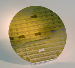
SiC technology on the advance. Structured SiC wafer. Fraunhofer IISB<br>
Including the Chair of Electron Devices of the University of Erlangen-Nuremberg, Germany, and CEMES-CNRS, Toulouse, France, the alliance covers all aspects of research and demonstrator development and makes the respective facilities available to third parties in cooperative projects.
The further development of novel “green” energy sources like wind or solar energy parks and a significant reduction of the world-wide energy consumption are of utmost importance for the reduction of CO2 emission. This includes the transition from conventional gasoline engines to electric or hybrid electric vehicles in automotive engineering. For all applications involving the transport of energy from power plants to the user, power management in cars, and conversion of energy, power electronic devices play an essential role.
Power devices based on materials with a wide energy bandgap such as silicon carbide and gallium nitride show the capability to overcome the material-dependent limits of today's power electronic devices based on silicon. Thereby, they will contribute essentially to the minimization of power dissipation.
In order to facilitate the development and take-up of this technology, and based on an existing cooperation formed within the Programme Inter Carnot Fraunhofer (PICF 2010), the Fraunhofer Institute for Integrated Systems and Device Technology IISB and the CNRS institute Laboratoire d'Analyse et d'Architecture des Systèmes (LAAS) together with their associates, the Chair of Electron Devices of the University Erlangen-Nuremberg (LEB) and the CNRS institute Centre d’Elaboration de Matériaux et d’Etudes Structurales (CEMES), formed the Wide Bandgap Semicon-ductor Alliance (WISEA). Together, the partners are able to offer a competence chain in wide bandgap semiconductor processing covering all aspects of research and demonstrator development.
WISEA has access to a 1000 m2 class-10 cleanroom in Erlangen, Germany, and to a 1500 m2 class-100 clean room in Toulouse, France, dedicated to micro and nanofabrication. In particular for wide bandgap semiconductor materials and devices, specialized equipment is available to cover processing from epitaxy to metallization and packaging, including the fabrication of test structures and devices. Based on its experienced staff and state-of-the-art facilities, the alliance also offers advanced electrical and physico-chemical characterization as well as simulation and modeling from atomistic processes to the device level.
The WISEA facilities are available for contract research as well as for third-party-funded collaborative projects.
WISEA acknowledges the initial support by the Federal Ministry of Education and Research (BMBF) of Germany and the Agence Nationale de la Recherche (ANR) of France within the Programme Inter Carnot Fraunhofer (PICF 2010) project MobiSiC.
WISEA is supported via the project MobiSiC by Federal Ministry of Education and Research (BMBF), The French National Research Agency (ANR), and the Carnot Institutes Network (Association Instituts Carnot).
Contact:
Dr. Anton J. Bauer
Fraunhofer Institute for Integrated Systems and Device Technology IISB
Schottkystrasse 10
91058 Erlangen, Germany
Tel. +49 9131 761 – 308
Fax +49 9131 761 – 360
anton.bauer@iisb.fraunhofer.de
www.iisb.fraunhofer.de
Dr. Fuccio Cristiano
LAAS-CNRS
7, avenue du Colonel Roche
31077 Toulouse Cedex 4, France
Tel. +33 5.61.33.62.54
Fax +33 5.61.33.62.08
fuccio@laas.fr
www.laas.fr
Fraunhofer IISB
The Institute for Integrated Systems and Device Technology IISB is one of the 59 institutes of the Fraunhofer-Gesellschaft. It conducts applied research and development in the fields of micro and nanoelectronics, power electronics, and mechatronics.
For the development of technology, equipment, and materials for nanoelectronics and its work on power electronic systems for energy efficiency, hybrid and electric cars the institute is internationally acknowledged.
A staff of 170 works in contract research for industry and public authorities. In addition to its headquarters in Erlangen, the IISB has two branch labs in Nuremberg and Freiberg.
The institute closely cooperates with the Chair of Electron Devices of the Friedrich-Alexander Universi-ty Erlangen-Nuremberg.
LAAS-CEMES/CNRS
The French national research centre for scientific research (CNRS), is a public research organization whose mission is to produce knowledge and make it available to society. LAAS and CEMES, both located in Toulouse, are two among its over 1000 research units spread throughout the country.
LAAS (Laboratoire d'Analyse et d'Architecture des Systèmes) gathers ~180 staff scientists (from both CNRS and Université Paul Sabatier, Toulouse), 90 engineers and 150 PhD students and post-docs working on five main areas: Microelectronics, Automatic Control, Computer Science, Production Con-trol, and Robotics. The laboratory clean room facility (1500 m2) includes conventional equipment for microelectronic and microsystems fabrication (e-beam pattern generator, mask patterning equipment, 200 keV ion implanter, RIE and CVD systems…).
CEMES (Centre d'Elaboration de Matériaux et d'Etudes Structurales) is devoted to the synthesis and structural characterisation of novel materials of small dimensions. About 70 staff scientists, physicists, materials scientists and chemists work together with 50 engineers and 30 PhD students and Postdocs in the field of materials sciences. These materials range from single molecules for electronic transfer to semiconductors, magnetic materials, ceramics, etc… to light alloys for aeronautics.
Media Contact
More Information:
http://www.iisb.fraunhofer.de/mobisicAll latest news from the category: Power and Electrical Engineering
This topic covers issues related to energy generation, conversion, transportation and consumption and how the industry is addressing the challenge of energy efficiency in general.
innovations-report provides in-depth and informative reports and articles on subjects ranging from wind energy, fuel cell technology, solar energy, geothermal energy, petroleum, gas, nuclear engineering, alternative energy and energy efficiency to fusion, hydrogen and superconductor technologies.


Newest articles

Properties of new materials for microchips
… can now be measured well. Reseachers of Delft University of Technology demonstrated measuring performance properties of ultrathin silicon membranes. Making ever smaller and more powerful chips requires new ultrathin…

Floating solar’s potential
… to support sustainable development by addressing climate, water, and energy goals holistically. A new study published this week in Nature Energy raises the potential for floating solar photovoltaics (FPV)…

Skyrmions move at record speeds
… a step towards the computing of the future. An international research team led by scientists from the CNRS1 has discovered that the magnetic nanobubbles2 known as skyrmions can be…

