Simplifying solar cells with a new mix of materials
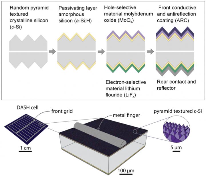
In this illustration, the top images show a cross-section of a solar cell design, called DASH, that uses a combination of moly oxide and lithium fluoride. This combination of materials allows the device to achieve high efficiency in converting sunlight to energy without the need for a process known as doping. The bottom images shows the dimensions of the DASH solar cell components. Credit: (Nature Energy: 10.1038/nenergy.2015.31)
An international research team has simplified the steps to create highly efficient silicon solar cells by applying a new mix of materials to a standard design. Arrays of solar cells are used in solar panels to convert sunlight to electricity.
The special blend of materials–which could also prove useful in semiconductor components–eliminates the need for a process known as doping that steers the device's properties by introducing foreign atoms to its electrical contacts. This doping process adds complexity to the device and can degrade its performance.
“The solar cell industry is driven by the need to reduce costs and increase performance,” said James Bullock, the lead author of the study, published this week in Nature Energy. Bullock participated in the study as a visiting researcher at the U.S. Department of Energy's Lawrence Berkeley National Laboratory (Berkeley Lab) and UC Berkeley.
“If you look at the architecture of the solar cell we made, it is very simple,” said Bullock, of Australian National University (ANU). “That simplicity can translate to reduced cost.”
Other scientists from Berkeley Lab, UC Berkeley, ANU and The Swiss Federal Institute of Technology of Lausanne (EPFL) also participated in the study.
Bullock added, “Conventional silicon solar cells use a process called impurity doping, which does bring about a number of limitations that are making further progress increasingly difficult.”
Most of today's solar cells use crystalline silicon wafers. The wafer itself, and sometimes the layers deposited on the wafer, are doped with atoms that either have electrons to spare when they bond with silicon atoms, or alternatively generate electron deficiencies, or “holes.” In both cases, this doping enhances electrical conductivity.
In these devices, two types of dopant atoms are required at the solar cell's electrical contacts to regulate how the electrons and holes travel in a solar cell so that sunlight is efficiently converted to electrical current that flows out of the cell.
Crystalline silicon-based solar cells with doped contacts can exceed 20 percent efficiency–meaning more than 20 percent of the sun's energy is converted to electricity. A dopant-free silicon cell had not previously exceeded 14 percent efficiency.
The new study, though, demonstrated a dopant-free silicon cell, referred to as a DASH cell (dopant free asymmetric heterocontact), with an average efficiency above 19 percent. This increased efficiency is a product of the new materials and a simple coating process for layers on the top and bottom of the device. Researchers showed it's possible to create their solar cell in just seven steps.
In this study, the research team used a crystalline silicon core (or wafer) and applied layers of dopant-free type of silicon called amorphous silicon.
Then, they applied ultrathin coatings of a material called molybdenum oxide, also known as moly oxide, at the sun-facing side of the solar cell, and lithium fluoride at the bottom surface. The two layers, having thicknesses of tens of nanometers, act as dopant-free contacts for holes and electrons, respectively.
“Moly oxide and lithium fluoride have properties that make them ideal for dopant-free electrical contacts,” said Ali Javey, program leader of Electronic Materials at Berkeley Lab and a professor of Electrical Engineering and Computer Sciences at UC Berkeley.
Both materials are transparent, and they have complementary electronic structures that are well-suited for solar cells.
“They were previously explored for other types of devices, but they were not carefully explored by the crystalline silicon solar cell community,” said Javey, the lead senior author of the study.
Javey noted that his group had discovered the utility of moly oxide as an efficient hole contact for crystalline silicon solar cells a couple of years ago. “It has a lot of defects, and these defects are critical and important for the arising properties. These are good defects,” he said.
Stefaan de Wolf, another author who is team leader for crystalline silicon research at EPFL in Neuchâtel, Switzerland, said, “We have adapted the technology in our solar cell manufacturing platform at EPFL and found out that these moly oxide layers work extremely well when optimized and used in combination with thin amorphous layer of silicon on crystalline wafers. They allow amazing variations of our standard approach.”
In the study, the team identified lithium fluoride as a good candidate for electron contacts to crystalline silicon coated with a thin amorphous layer. That layer complements the moly oxide layer for hole contacts.
The team used a room-temperature technique called thermal evaporation to deposit the layers of lithium fluoride and moly oxide for the new solar cell. There are many other materials that the research teams hopes to test to see if they can improve the cell's efficiency.
Javey said there is also promise for adapting the material mix used in the solar cell study to improve the performance of semiconductor transistors. “There's a critical need to reduce the contact resistance in transistors so we're trying to see if this can help.”
###
Some off the work in this study was performed at The Molecular Foundry, a DOE Office of Science User Facility at Berkeley Lab.
This work was supported by the DOE Office of Science, Bay Area Photovoltaics Consortium (BAPVC); the Joint Center for Artificial Photosynthesis, a DOE Energy Innovation Hub; Office fédéral de l'énergie (OFEN); the Australian Renewable Energy Agency (ARENA) and the CSEM PV-center.
More information about Ali Javey's research is available here: http://nano.
Lawrence Berkeley National Laboratory addresses the world's most urgent scientific challenges by advancing sustainable energy, protecting human health, creating new materials, and revealing the origin and fate of the universe. Founded in 1931, Berkeley Lab's scientific expertise has been recognized with 13 Nobel prizes. The University of California manages Berkeley Lab for the U.S. Department of Energy's Office of Science. For more, visit http://www.
The DOE Office of Science is the single largest supporter of basic research in the physical sciences in the United States and is working to address some of the most pressing challenges of our time. For more information, please visit science.energy.gov.
Media Contact
All latest news from the category: Power and Electrical Engineering
This topic covers issues related to energy generation, conversion, transportation and consumption and how the industry is addressing the challenge of energy efficiency in general.
innovations-report provides in-depth and informative reports and articles on subjects ranging from wind energy, fuel cell technology, solar energy, geothermal energy, petroleum, gas, nuclear engineering, alternative energy and energy efficiency to fusion, hydrogen and superconductor technologies.


Newest articles

Silicon Carbide Innovation Alliance to drive industrial-scale semiconductor work
Known for its ability to withstand extreme environments and high voltages, silicon carbide (SiC) is a semiconducting material made up of silicon and carbon atoms arranged into crystals that is…

New SPECT/CT technique shows impressive biomarker identification
…offers increased access for prostate cancer patients. A novel SPECT/CT acquisition method can accurately detect radiopharmaceutical biodistribution in a convenient manner for prostate cancer patients, opening the door for more…

How 3D printers can give robots a soft touch
Soft skin coverings and touch sensors have emerged as a promising feature for robots that are both safer and more intuitive for human interaction, but they are expensive and difficult…

