Research discovery could revolutionise semiconductor manufacture
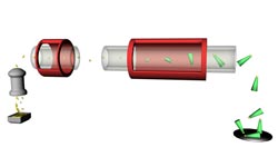
Image: Aerotaxy production process<br>
Instead of starting from a silicon wafer or other substrate, as is usual today, researchers have made it possible for the structures to grow from freely suspended nanoparticles of gold in a flowing gas.
Behind the discovery is Lars Samuelson, Professor of Semiconductor Physics at Lund University, Sweden, and head of the University’s Nanometre Structure Consortium. He believes the technology will be ready for commercialisation in two to four years’ time. A prototype for solar cells is expected to be completed in two years.
“When I first suggested the idea of getting rid of the substrate, people around me said ‘you’re out of your mind, Lars; that would never work’. When we tested the principle in one of our converted ovens at 400°C, the results were better than we could have dreamt of”, he says.
“The basic idea was to let nanoparticles of gold serve as a substrate from which the semiconductors grow. This means that the accepted concepts really were turned upside down!”
Since then, the technology has been refined, patents have been obtained and further studies have been conducted. In the article in Nature, the researchers show how the growth can be controlled using temperature, time and the size of the gold nanoparticles.
Recently, they have also built a prototype machine with a specially built oven. Using a series of ovens, the researchers expect to be able to ‘bake’ the nanowires, as the structures are called, and thereby develop multiple variants, such as p-n diodes.
A further advantage of the technology is avoiding the cost of expensive semiconductor wafers.
“In addition, the process is not only extremely quick, it is also continuous. Traditional manufacture of substrates is batch-based and is therefore much more time-consuming”, adds Lars Samuelson.
At the moment, the researchers are working to develop a good method to capture the nanowires and make them self-assemble in an ordered manner on a specific surface. This could be glass, steel or another material suited to the purpose.
The reason why no one has tested this method before, in the view of Professor Samuelson, is that today’s method is so basic and obvious. Such things tend to be difficult to question.
However, the Lund researchers have a head start thanks to their parallel research based on an innovative method in the manufacture of nanowires on semiconductor wafers, known as epitaxy – consequently, the researchers have chosen to call the new method aerotaxy. Instead of sculpting structures out of silicon or another semiconductor material, the structures are instead allowed to develop, atomic layer by atomic layer, through controlled self-organisation.
The structures are referred to as nanowires or nanorods. The breakthrough for these semiconductor structures came in 2002 and research on them is primarily carried out at Lund, Berkeley and Harvard universities.
The Lund researchers specialise in developing the physical and electrical properties of the wires, which helps create better and more energy-saving solar cells, LEDs, batteries and other electrical equipment that is now an integrated part of our lives.
The article ‘Continuous gas-phase synthesis of nanowires with tuneable properties’ can be found by entering “I 10.1038/nature11652” here: http://dx.doi.org/.
Besides Lars Samuelson, the other authors of the article are: Magnus Heurlin, Martin Magnusson, David Lindgren, Martin Ek, Reine Wallenberg and Knut Deppert, all employed at Lund University, except for Martin Magnusson, who works at start-up company Sol Voltaics AB.
The research has been funded by the Swedish Research Council, the Swedish Foundation for Strategic Research (SSF), the Knut and Alice Wallenberg Foundation and Vinnova.
For more information, contact Lars Samuelson, +46 46 222 76 79, +46 703 17 76 79, Lars.Samuelson@ftf.lth.se.
Contact details for the other authors can be found by searching on www.lunduniversity.lu.se.
Lund University Nanometre Structure Consortium, nmC@LU: www.nano.lth.se.
About semiconductors
Semiconductors are materials that neither conduct electricity as well as metals, nor stop a current as effectively as insulators – silicon and germanium are two examples. These properties may not sound attractive, but in actual fact they are excellent. The reason is that we can influence the conductive capacity of the materials, for example by introducing impurity atoms, known as doping. Materials with different types of doping can be combined to manufacture products such as transistors, solar cells or LEDs.
Media Contact
More Information:
http://www.lu.seAll latest news from the category: Power and Electrical Engineering
This topic covers issues related to energy generation, conversion, transportation and consumption and how the industry is addressing the challenge of energy efficiency in general.
innovations-report provides in-depth and informative reports and articles on subjects ranging from wind energy, fuel cell technology, solar energy, geothermal energy, petroleum, gas, nuclear engineering, alternative energy and energy efficiency to fusion, hydrogen and superconductor technologies.


Newest articles

Properties of new materials for microchips
… can now be measured well. Reseachers of Delft University of Technology demonstrated measuring performance properties of ultrathin silicon membranes. Making ever smaller and more powerful chips requires new ultrathin…

Floating solar’s potential
… to support sustainable development by addressing climate, water, and energy goals holistically. A new study published this week in Nature Energy raises the potential for floating solar photovoltaics (FPV)…

Skyrmions move at record speeds
… a step towards the computing of the future. An international research team led by scientists from the CNRS1 has discovered that the magnetic nanobubbles2 known as skyrmions can be…

