Production nanophotonics – dream or reality?

Nanophotonics could well revolutionise the fields of telecommunications, computing and sensing, according to Professor Clivia Sotomayor Torres. But why is research into nanophotonics important?
It has the potential to provide ultra-small optoelectronic components, high speed and greater bandwidth. Professor Sotomayor Torres believes current research into fabricating nano-electronics could open the way for new methods of making nanophotonic devices, i.e. mass producing light handling devices that may be only tens or hundreds of nanometres in size that will help drive this revolution.
Sotomayor defines nanophotonics as the interactions that take place within the wavelength of the light scale or, in particular, within a sub-wavelength of light, and those that are modified by the nature of the material in the nanometre scale.
She says there is a need to understand how optics behave when molecules traverse clusters or metal particles. Researchers now have the tools, she says, to map topology and size with optical properties. In the past these tools were not available.
“Today we have some very genuine engineering concerns when producing ultra-compact, low-power optical devices; devices are highly sensitive, down to the level of single photon detection or emission, to the level of computation by molecules,” she says.
She states that we are just beginning to understand the behaviour of light in periodic media. “We have an understanding of what happens in periodic structures, and at the other end what happens in single molecules. The gap in between is what is missing. What happens when we have molecular arrays or clusters? The description of what happens in optical properties is not clear. It is not yet satisfactory. The whole area of light behaviour in complex media, materials with short-chain polymers for example. Structures of devices, platforms, substrates for example. We really know very little about light/matter interaction with such structures.”
The challenge – develop mass production techniques
We need to understand this area, she says, because to fabricate a test structure it is necessary to predetermine parameters. “The permutations are infinite, there are millions of molecules, millions of different atoms and things you can attach to them, the way you get order is also nearly infinite. So we need some window of parameters to help target our molecular samples into something that can give information on device-relevant properties.”
There are several challenges involved in developing fabrication techniques suitable for mass production, states Sotomayor. One is power consumption. Another is that of cost. The task is to work with molecules embedded in a matrix in a way that can be reproduced by the tonne, thus giving an advantage over current technologies.
Current fabrication methods are based on an expensive and highly toxic process called Metal Organic Chemical Vapour Deposition. “This is high-tech at a high price,” says Sotomayor. She doesn’t propose to use that.
Rather, with molecular photonics, researchers hope to develop methods of large-scale production that are more cost-effective and environmentally friendly, she says. “We are talking of self-assembly, working with polymers, working with matrices. This approach is now a laboratory method, tested with an output of a few milligrammes rather than many kilogrammes. But if we want to have devices in ten to twenty years from now, we will need to be able to produce kilos.”
So, she says, there is a need for preparation techniques that can be scaled up. “For example we don’t know yet what tolerances we will have to meet when it comes to material purity. This will be an important cost factor.”
The efficiency of energy transfer is also significant, she says. “Can we convert energy from a molecular transition into an electronic transition? Convert photons to electrons and back to photons? This has been done, but we don’t yet know how efficient such processes are. Nobody dares to talk about losses. We don’t have standards yet.”
Noting that existing electron/photon translators are very large, typically millimetres square, she says that, “We are working towards micrometres. We are trying to convert light so that it will go into metal islands a few nanometres in size. This is where the nanophotonics comes in. That is the conversion we have to do, otherwise we are stuck with 500 nanometres and a few microns still.”
Applications for the medium term…
Asked about likely application areas, Sotomayor replies that most people think about light source applications, ranging from flat-panel displays through electronic paper to detectors.
In the field of displays for example, “Basically you have to produce images that you control with liquid crystals or with fluorescent molecules,” she says. Ultimately this could result in the Internet displayed in people’s living rooms on a larger screen, with wallpaper acting as the display.
But that is the five-year timescale, she believes. “What we are most interested in is the ten – fifteen – twenty year timescale. Here nanophotonics can be a bridge between existing optoelectronic devices and future circuitry via an incremental incorporation of nanostructures.”
Nanophotonics, according to Sotomayor, has the potential to transform telecommunications technologies in a way even more radical than the emergence of integrated circuits. “We’re talking about applications like light emitters, light sources and light detectors. Components like waveguides – how to transmit light from A to B. And switches – we have a very good prospect in switching, because the optical properties of molecules are highly non-linear. And that is an essential condition for switching devices. So there are very clear applications, or device-relevant properties, here.”
…and the future
She notes, “If we go from nanophotonics to molecular photonics, this provides a link to developments in molecular electronics. For us that is especially important because of the smaller-size electronic devices being developed, which also have their properties determined by their molecular nature.”
“We have to bring together the advantages of molecular photonics with those of molecular electronics, based on the common molecular aspects for preparation, for handling, for lifetimes, etc. It may well be that molecular electronics is the electronics of the future.”
Having served on the management board of the IST-programme funded nanoelectronics Network of Excellence project, PHANTOMS, in addition to coordinating several national and international projects in nanofabrication and photonic crystals, she emphasises that the EU needs to invest to keep up, remarking that in the United States anything with the word ’nano’ tends to attract huge venture capital.
Contact:
Professor Clivia Sotomayor Torres
NMRC
’Lee Maltings’
Prospect Row
Cork
Ireland
Email: Clivia.sotomayor@nmrc.ie
Source: Based on interview with Professor Clivia Sotomayor Torres
Media Contact
All latest news from the category: Power and Electrical Engineering
This topic covers issues related to energy generation, conversion, transportation and consumption and how the industry is addressing the challenge of energy efficiency in general.
innovations-report provides in-depth and informative reports and articles on subjects ranging from wind energy, fuel cell technology, solar energy, geothermal energy, petroleum, gas, nuclear engineering, alternative energy and energy efficiency to fusion, hydrogen and superconductor technologies.
Newest articles

Properties of new materials for microchips
… can now be measured well. Reseachers of Delft University of Technology demonstrated measuring performance properties of ultrathin silicon membranes. Making ever smaller and more powerful chips requires new ultrathin…

Floating solar’s potential
… to support sustainable development by addressing climate, water, and energy goals holistically. A new study published this week in Nature Energy raises the potential for floating solar photovoltaics (FPV)…

Skyrmions move at record speeds
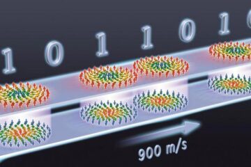
… a step towards the computing of the future. An international research team led by scientists from the CNRS1 has discovered that the magnetic nanobubbles2 known as skyrmions can be…


