Photonics: Better connected

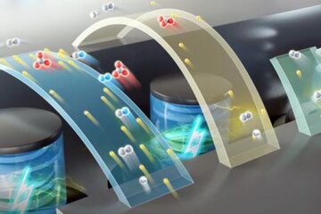
Silicon is a unique material that has revolutionized electronics; it enables engineers to put millions of electrical devices onto a single chip. Replacing the electrical currents in this technology with beams of light could enable even faster information processing. Qian Wang at the A*STAR Data Storage Institute and co-workers1 have now designed a crucial component for such optical chips — a connector that links the silicon chip to an optical fiber. Such a device should enable efficient light input and output.
Silicon is a promising platform for dense photonic integration because sub-micrometer-sized silicon wires, known as waveguides, are capable of tightly confining and guiding light. As the technology required for processing silicon in this way already exists, silicon nanowires are attracting attention from the electronics industry. The challenge, however, is to be able to insert and extract a beam of light efficiently into and out of such tiny structures.
Wang and his team have now designed an ultra-compact lens that can be directly integrated into the silicon chip at the end of the waveguide. Their proposed lens is based on an idea known as a graded refractive index (GRIN) lens. The common GRIN lens usually distorts a light beam as it is collimated or focused, resulting in a so-called aberration. “We now propose a computational algorithm that can generate a novel graded refractive index profile for the GRIN lens and thus achieve aberration-free sub-wavelength focusing and highly efficient coupling,” says Wang.
The team of researchers’ graded index structure consists of a stack of alternating layers of two materials — for example, using silicon, which has a high refractive index, and silicon dioxide, which has a low refractive index. The layers of silicon are thicker than those of silicon dioxide at the optical axis, but this gradually reverses higher up in the stack.
Simulations showed how this structure could expand out light travelling along a 300 nanometer-thick silicon waveguide so that it couples to a fiber with a diameter of 10.4 micrometers. With appropriate anti-reflection coating, the coupling efficiency was calculated to be as high as 90%. The team of researchers also assessed the sensitivity of the optical coupling to any movement of the fiber, indicating that the new approach would provide a compact, efficient and robust way of achieving fiber-to-nanophotonic chip coupling. The next step will be to demonstrate this concept experimentally. “We plan to incorporate the idea into an electronic–photonic integration platform,” says Wang.
The A*STAR-affiliated researchers contributing to this research are from the Data Storage Institute
Media Contact
All latest news from the category: Power and Electrical Engineering
This topic covers issues related to energy generation, conversion, transportation and consumption and how the industry is addressing the challenge of energy efficiency in general.
innovations-report provides in-depth and informative reports and articles on subjects ranging from wind energy, fuel cell technology, solar energy, geothermal energy, petroleum, gas, nuclear engineering, alternative energy and energy efficiency to fusion, hydrogen and superconductor technologies.
Newest articles

High-energy-density aqueous battery based on halogen multi-electron transfer
Traditional non-aqueous lithium-ion batteries have a high energy density, but their safety is compromised due to the flammable organic electrolytes they utilize. Aqueous batteries use water as the solvent for…

First-ever combined heart pump and pig kidney transplant
…gives new hope to patient with terminal illness. Surgeons at NYU Langone Health performed the first-ever combined mechanical heart pump and gene-edited pig kidney transplant surgery in a 54-year-old woman…

Biophysics: Testing how well biomarkers work
LMU researchers have developed a method to determine how reliably target proteins can be labeled using super-resolution fluorescence microscopy. Modern microscopy techniques make it possible to examine the inner workings…


