One-dimensional material packs a powerful punch for next generation electronics
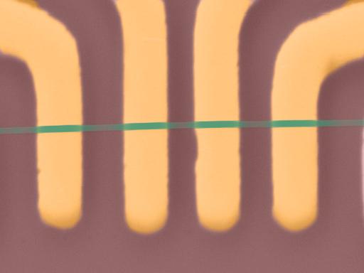
Microscopy image of an electronic device made with 1D ZrTe3 nanoribbons. The nanoribbon channel is indicated in green color. The metal contacts are shown in yellow color. Note than owing to the nanometer scale thickness the yellow metal contacts appear to be under the green channel while in reality they are on top Credit: Balandin lab, UC Riverside
Engineers at the University of California, Riverside, have demonstrated prototype devices made of an exotic material that can conduct a current density 50 times greater than conventional copper interconnect technology.
Current density is the amount of electrical current per cross-sectional area at a given point. As transistors in integrated circuits become smaller and smaller, they need higher and higher current densities to perform at the desired level. Most conventional electrical conductors, such as copper, tend to break due to overheating or other factors at high current densities, presenting a barrier to creating increasingly small components.
The electronics industry needs alternatives to silicon and copper that can sustain extremely high current densities at sizes of just a few nanometers.
The advent of graphene resulted in a massive, worldwide effort directed at investigation of other two-dimensional, or 2D, layered materials that would meet the need for nanoscale electronic components that can sustain a high current density. While 2D materials consist of a single layer of atoms, 1D materials consist of individual chains of atoms weakly bound to one another, but their potential for electronics has not been as widely studied.
One can think of 2D materials as thin slices of bread while 1D materials are like spaghetti. Compared to 1D materials, 2D materials seem huge.
A group of researchers led by Alexander A. Balandin, a distinguished professor of electrical and computer engineering in the Marlan and Rosemary Bourns College of Engineering at UC Riverside, discovered that zirconium tritelluride, or ZrTe3, nanoribbons have an exceptionally high current density that far exceeds that of any conventional metals like copper.
The new strategy undertaken by the UC Riverside team pushes research from two-dimensional to one-dimensional materials– an important advance for the future generation of electronics.
“Conventional metals are polycrystalline. They have grain boundaries and surface roughness, which scatter electrons,” Balandin said. “Quasi-one-dimensional materials such as ZrTe3 consist of single-crystal atomic chains in one direction. They do not have grain boundaries and often have atomically smooth surfaces after exfoliation. We attributed the exceptionally high current density in ZrTe3 to the single-crystal nature of quasi-1D materials.”
In principle, such quasi-1D materials could be grown directly into nanowires with a cross-section that corresponds to an individual atomic thread, or chain. In the present study the level of the current sustained by the ZrTe3 quantum wires was higher than reported for any metals or other 1D materials. It almost reaches the current density in carbon nanotubes and graphene.
Electronic devices depend on special wiring to carry information between different parts of a circuit or system. As developers miniaturize devices, their internal parts also must become smaller, and the interconnects that carry information between parts must become smallest of all. Depending on how they are configured, the ZrTe3 nanoribbons could be made into either nanometer-scale local interconnects or device channels for components of the tiniest devices.
The UC Riverside group's experiments were conducted with nanoribbons that had been sliced from a pre-made sheet of material. Industrial applications need to grow nanoribbon directly on the wafer. This manufacturing process is already under development, and Balandin believes 1D nanomaterials hold possibilities for applications in future electronics.
“The most exciting thing about the quasi-1D materials is that they can be truly synthesized into the channels or interconnects with the ultimately small cross-section of one atomic thread– approximately one nanometer by one nanometer,” Balandin said.
###
The results of this investigation appear this month in IEEE Electron Device Letters [see A. Geremew, M. A. Bloodgood, E. Aytan, B. W. K. Woo, S. R. Corber, G. Liu, K. Bozhilov, T. T. Salguero, S. Rumyantsev, M. P. Rao, and A. A. Balandin, “Current Carrying Capacity of Quasi-1DZrTe3 van der Waals Nanoribbons,” IEEE, Electron. Device Lett., 39, 735 (2018).
Adane Geremew, the first author of the paper, is a Ph.D. student in Balandin's group. Professor Tina Salguero, University of Georgia, synthesized the bulk materials, which were used for exfoliation of nanoribbons.
The research was supported by the Semiconductor Research Corporation and the National Science Foundation.
The University of California, Riverside (http://www.
Media Contact
All latest news from the category: Power and Electrical Engineering
This topic covers issues related to energy generation, conversion, transportation and consumption and how the industry is addressing the challenge of energy efficiency in general.
innovations-report provides in-depth and informative reports and articles on subjects ranging from wind energy, fuel cell technology, solar energy, geothermal energy, petroleum, gas, nuclear engineering, alternative energy and energy efficiency to fusion, hydrogen and superconductor technologies.


Newest articles
Making diamonds at ambient pressure
Scientists develop novel liquid metal alloy system to synthesize diamond under moderate conditions. Did you know that 99% of synthetic diamonds are currently produced using high-pressure and high-temperature (HPHT) methods?[2]…

Eruption of mega-magnetic star lights up nearby galaxy
Thanks to ESA satellites, an international team including UNIGE researchers has detected a giant eruption coming from a magnetar, an extremely magnetic neutron star. While ESA’s satellite INTEGRAL was observing…
Solving the riddle of the sphingolipids in coronary artery disease
Weill Cornell Medicine investigators have uncovered a way to unleash in blood vessels the protective effects of a type of fat-related molecule known as a sphingolipid, suggesting a promising new…

