OLED: Nanometer-thin layer improves efficiency
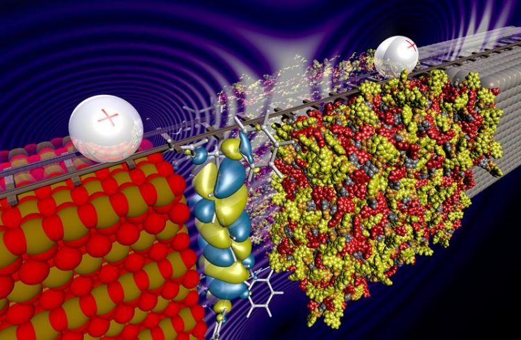
Visualization of a current through an OLED, flowing via a thin molecular layer (center) from an electrode (left) to an organic semiconductor (right). Copyright: Max Planck Institute for Polymer Research
Organic light-emitting diodes (OLEDs) are used as light sources in high-quality smartphone displays and large-area high-end products such as OLED televisions. The main active component in an OLED is a light-emitting layer of an organic semiconductor, which converts electrical energy into visible light.
In an OLED, the organic semiconducting layer is situated between two electrodes; by applying a voltage across these two electrodes, an electric current passes through the OLED, which is converted into visible light.
However, for many organic semiconductors, especially for blue- or ultraviolet-emitting materials, it is difficult to inject the current from the positive electrode into the OLED. This leads to low efficiencies in OLEDs.
Dr. Gert-Jan Wetzelaer, Group Leader at the Max Planck Institute for Polymer Research in Mainz, Germany, has recently discovered a way of improving the current injection from the positive electrode in OLEDs. Wetzelaer and his team have covered the positive electrode with an ultrathin layer of another organic semiconductor as a spacer layer between the electrode and the light-emitting organic semiconductor.
Wetzelaer said: “The result was unexpected. This nanometer-thin layer facilitates charge transfer between the electrode and the organic semiconductor. Although it seems to be illogical at first, eliminating physical contact between electrode and semiconductor actually improves the electrical contact.”
Improved contacts in semiconductors
Improving electrical contact with an ultrathin interlayer greatly increases the efficiency of ultraviolet-emitting OLEDs. The scientists at the MPI for Polymer Research have demonstrated this improvement of electrodes for a large number of organic semiconductors and for different spacer layers.
Professor Paul Blom, Director at the Max Planck Institute for Polymer Research and head of its Molecular Electronics Department, is convinced: “This simple method of covering electrodes in OLEDs with an ultrathin layer for current-injection improvement is a resounding success for technical application in high-end electronics.”
Gert-Jan Wetzelaer and his research team are very confident that this new approach for fabricating improved contacts can be used in basically any organic-semiconductor device, which could boost their performance now.
Original article:
Naresh B. Kotadiya, Hao Lu, Anirban Mondal, Yutaka Ie, Denis Andrienko, Paul W. M. Blom & Gert-Jan A. H. Wetzelaer: Universal strategy for Ohmic hole injection into organic semiconductors with high ionization energies.
Nature Materials (2018)
DOI:10.1038/s41563-018-0022-8
About the Max Planck Institute for Polymer Research:
The Max Planck Institute for Polymer Research (MPI-P) ranks among the globally leading research centers in the field of polymer research since its foundation in 1984. The focus on soft materials and macromolecular materials has resulted in the worldwide unique position of the MPI-P and its research focus. Fundamental polymers research on both production and characterization as well as analysis of physical and chemical properties are conducted by scientific collaborators from all over the world. Presently over 500 people are working at the MPI-P, the vast majority of whom are engaged in scientific research.
http://www.mpip-mainz.mpg.de/home/en
http://www.mpip-mainz.mpg.de/5269530/pm2018-07
https://www.nature.com/articles/s41563-018-0022-8
Media Contact
All latest news from the category: Power and Electrical Engineering
This topic covers issues related to energy generation, conversion, transportation and consumption and how the industry is addressing the challenge of energy efficiency in general.
innovations-report provides in-depth and informative reports and articles on subjects ranging from wind energy, fuel cell technology, solar energy, geothermal energy, petroleum, gas, nuclear engineering, alternative energy and energy efficiency to fusion, hydrogen and superconductor technologies.


Newest articles

Properties of new materials for microchips
… can now be measured well. Reseachers of Delft University of Technology demonstrated measuring performance properties of ultrathin silicon membranes. Making ever smaller and more powerful chips requires new ultrathin…

Floating solar’s potential
… to support sustainable development by addressing climate, water, and energy goals holistically. A new study published this week in Nature Energy raises the potential for floating solar photovoltaics (FPV)…

Skyrmions move at record speeds
… a step towards the computing of the future. An international research team led by scientists from the CNRS1 has discovered that the magnetic nanobubbles2 known as skyrmions can be…

