New method monitors semiconductor etching as it happens ' with light

“You can use light to image the topography and you can use light to sculpture the topography,” said electrical and computer engineering professor Gabriel Popescu. “That’s the future of semiconductor etching.”
Chip makers and semiconductor researchers need to very precisely control the dimensions of their devices. The dimensions of the components affect performance, speed, error rate and time to failure.
Semiconductors are commonly shaped by etching with chemicals. Etching errors, such as residual layers, can affect the ability to further process and etch as well as hamper device performance. Thus, researchers use time-consuming and costly processes to ensure precise etching – for some applications, to within a scant few nanometers.
The Illinois researchers’ new technique can monitor a semiconductor’s surface as it is etched, in real time, with nanometer resolution. It uses a special type of microscope that uses two beams of light to very precisely measure topography.
“The idea is that the height of the structure can be determined as the light reflects off the different surfaces,” said electrical and computer engineering professor Lynford Goddard, who co-led the group with Popescu. “Looking at the change in height, you figure out the etch rate. What this allows us to do is monitor it while it’s etching. It allows us to figure out the etch rate both across time and across space, because we can determine the rate at every location within the semiconductor wafer that’s in our field of view.”
The new method is faster, lower in cost, and less noisy than the widely used methods of atomic force microscopy or scanning tunneling microscopy, which cannot monitor etching in progress but only compare before and after measurements. In addition, the new method is purely optical, so there’s no contact with the semiconductor surface and the researchers can monitor the whole wafer at once instead of point-by-point.
“I would say the main advantage of an optical technique is that it requires no contact,” Popescu said. “We’re just sending light, reflected off the sample, as opposed to an AFM where you need to come with a probe close to the sample.”
In addition to monitoring the etching process, the light catalyzes the etching process itself, called photochemical etching. Traditional chemical etching creates features in steps or plateaus. For curved surfaces or other shapes, semiconductor researchers use photochemical etching.
Usually, light shines though very expensive glass plates called masks that have distinct patterns of gray to let light through by degrees. A researcher must purchase or make a mask for each tweak of a pattern until the correct pattern of features is achieved.
By contrast, the new method uses a projector to shine a grayscale image onto the sample being etched. This allows the researchers to create complex patterns quickly and easily, and adjust them as needed.
“To create each mask is very expensive. That’s impractical for research,” Goddard said. “Because our technique is controlled by the computer, it can be dynamic. So you can start off etching one particular shape, midway through realize that you want to make some change, and then change the projector pattern to get the desired outcome.“
The researchers envision this technology applied beyond etching, to real-time monitoring of other processes in materials science and life science – for example, watching carbon nanotubes self-assemble, or error monitoring during large-scale computer chip manufacturing. It could help chip manufacturers reduce costs and processing time by ensuring that equipment stays calibrated.
The National Science Foundation supported this work, published Sept. 28 in the journal Light: Science and Applications. Goddard and Popescu are also affiliated with the Beckman Institute for Advanced Science and Technology at the U. of I.
Graduate students Chris Edwards and Amir Arbabi were also co-authors of the paper.
Editor’s notes: To reach Lynford Goddard, call 217-244-0799; email lgoddard@illinois.edu.
To reach Gabriel Popescu, 217-333-4840; gpopescu@illinois.edu.
The paper, “Optically Monitoring and Controlling Nanoscale Topography During Semiconductor Etching,” is available online
http://www.nature.com/lsa/journal/v1/n9/full/lsa201230a.html
See a video of Goddard explain the etching metho
http://news.illinois.edu/videos.html?destinationID=vmGiOUsYPk2IJcKSvIjqAA&contentID=eAyGTzoH7UeRk6CiNGW2SA
Media Contact
More Information:
http://www.illinois.eduAll latest news from the category: Power and Electrical Engineering
This topic covers issues related to energy generation, conversion, transportation and consumption and how the industry is addressing the challenge of energy efficiency in general.
innovations-report provides in-depth and informative reports and articles on subjects ranging from wind energy, fuel cell technology, solar energy, geothermal energy, petroleum, gas, nuclear engineering, alternative energy and energy efficiency to fusion, hydrogen and superconductor technologies.
Newest articles
Superradiant atoms could push the boundaries of how precisely time can be measured
Superradiant atoms can help us measure time more precisely than ever. In a new study, researchers from the University of Copenhagen present a new method for measuring the time interval,…
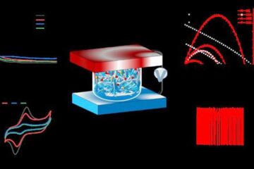
Ion thermoelectric conversion devices for near room temperature
The electrode sheet of the thermoelectric device consists of ionic hydrogel, which is sandwiched between the electrodes to form, and the Prussian blue on the electrode undergoes a redox reaction…
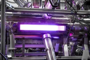
Zap Energy achieves 37-million-degree temperatures in a compact device
New publication reports record electron temperatures for a small-scale, sheared-flow-stabilized Z-pinch fusion device. In the nine decades since humans first produced fusion reactions, only a few fusion technologies have demonstrated…


