Metalens grows up
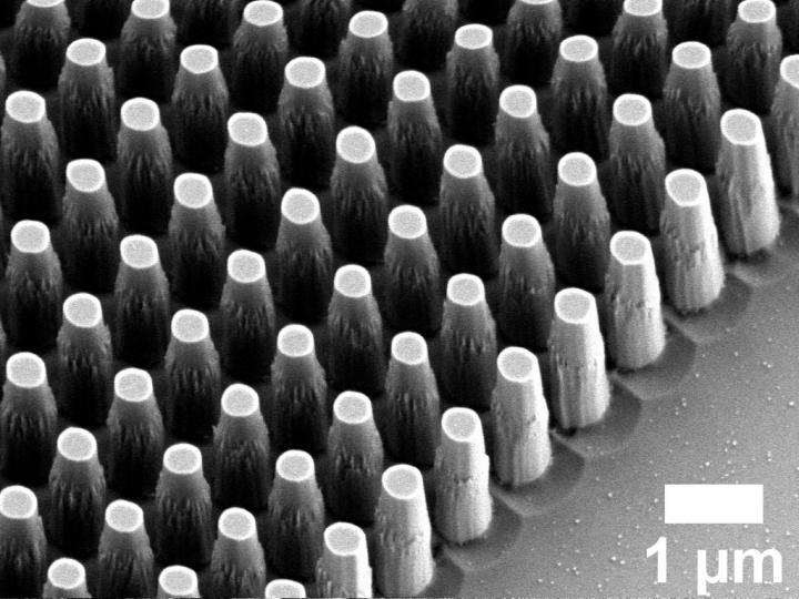
This is a zoomed-in SEM image of nanopillars of the metalens. (Image courtesy of Joon-Suh Park/Harvard SEAS)
Metalenses — flat surfaces that use nanostructures to focus light — are poised to revolutionize everything from microscopy to cameras, sensors, and displays. But so far, most of the lenses have been about the size of a piece of glitter.
While lenses this size work well for some applications, a larger lens is needed for low-light conditions, such as an imaging system onboard orbital satellites, and VR applications, where the lens needs to be larger than a pupil.
Now, researchers at the Harvard John A. Paulson School of Engineering and Applied Sciences (SEAS) have developed an all-glass, centimeter-scale metalens in the visible spectrum that can be manufactured using conventional chip fabrication methods.
The research was published in Nano Letters.
“This research paves the way for so-called wafer level cameras for cell phones, where the CMOS chip and the metalenses can be directly stacked on top of each other with easy optical alignment because they are both flat,” said Federico Capasso, the Robert L. Wallace Professor of Applied Physics and Vinton Hayes Senior Research Fellow in Electrical Engineering at SEAS and senior author of the paper. “In the future, the same company can make both the chip and the lenses because both can be made using the same technology: lithography.”
“Previously, we were not able to achieve mass-production of centimeter-scale metalenses at visible wavelengths because we were either using electron-beam lithography, which is too time consuming, or a technique called i-line stepper lithography, which does not have enough resolution to pattern the required subwavelength-sized structures,” said Joon-Suh Park, a Ph.D. candidate at SEAS and first author of the paper.
To mass produce a centimeter-scale metalens, the researchers used a technique called deep-ultraviolet (DUV) projection lithography, which is commonly used to pattern very fine lines and shapes in silicon chips in everything from computers to cell phones. The technique can produce many metalenses per chip, each made of millions of nanoscale elements with a single shot of exposure, like taking a photograph.
The researchers eliminated the time-consuming deposition processes that were required for previous metalenses by etching the nanostructure pattern directly onto a glass surface.
It is the first mass-producible, all-glass, centimeter-scale metalens in the visible spectrum.
While this lens is chromatic, meaning all the different colors of light don't focus at the same spot, the researchers are working on large-diameter achromatic metalenses.
###
The research was co-authored by Shuyan Zhang, Alan She, Wei Ting Chen, Peng Lin, Kerolos M. A. Yousef, and Ji-Xin Cheng and supported in part by the Defense Advanced Research Projects Agency.
This work was performed in part at the Cornell NanoScale Science & Technology Facility and the Center for Nanoscale Systems at Harvard University, both of which are members of the National Nanotechnology Coordinated Infrastructure (NNCI), which is supported by the National Science Foundation.
Media Contact
More Information:
https://www.seas.harvard.edu/news/2019/12/metalens-growsAll latest news from the category: Power and Electrical Engineering
This topic covers issues related to energy generation, conversion, transportation and consumption and how the industry is addressing the challenge of energy efficiency in general.
innovations-report provides in-depth and informative reports and articles on subjects ranging from wind energy, fuel cell technology, solar energy, geothermal energy, petroleum, gas, nuclear engineering, alternative energy and energy efficiency to fusion, hydrogen and superconductor technologies.


Newest articles

Solving the riddle of the sphingolipids in coronary artery disease
Weill Cornell Medicine investigators have uncovered a way to unleash in blood vessels the protective effects of a type of fat-related molecule known as a sphingolipid, suggesting a promising new…
Rocks with the oldest evidence yet of Earth’s magnetic field
The 3.7 billion-year-old rocks may extend the magnetic field’s age by 200 million years. Geologists at MIT and Oxford University have uncovered ancient rocks in Greenland that bear the oldest…
Decisive breakthrough for battery production
Storing and utilising energy with innovative sulphur-based cathodes. HU research team develops foundations for sustainable battery technology Electric vehicles and portable electronic devices such as laptops and mobile phones are…

