Illinois team advances GaN-on-Silicon for scalable high electron mobility transistors
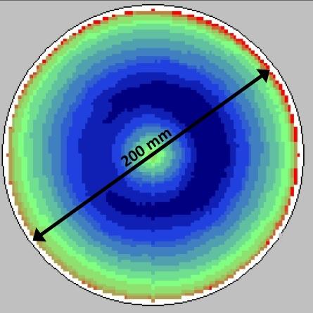
This is a GaN on 200 mm Si wafer thickness mapping image. Credit: University of Illinois
Can Bayram, an assistant professor of electrical and computer engineering (ECE), and his team have created the GaN HEMT structure on a silicon platform because it is compatible with existing CMOS manufacturing processes and is less expensive than other substrate options like sapphire and silicon carbide.
However, silicon does have its challenges. Namely, the lattice constant, or space between silicon atoms, doesn't match up with the atomic structure of the GaN grown on top of it.
“When you grow the GaN on top, there's a lot of strain between the layers, so we grew buffer layers [between the silicon and GaN] to help change the lattice constant into the proper size,” explained ECE undergraduate researcher Josh Perozek, lead author of the group's paper, “Investigation of structural, optical, and electrical characteristics of an AlGaN/GaN high electron mobility transistor structure across a 200mm Si(1 1 1) substrate,” in the Journal of Physics D: Applied Physics.
Without these buffer layers, cracks or other defects will form in the GaN material, which would prevent the transistor from operating properly. Specifically, these defects — threading dislocations or holes where atoms should be–ruin the properties of the 2-dimensional electron gas channel in the device. This channel is critical to the HEMTs ability to conduct current and function at high frequencies.
“The single most important thing for these GaN [HEMT] devices is to have high 2D electron gas concentration,” said Bayram, about the accumulation of electrons in a channel at the interface between the silicon and the various GaN-based layers above it.
“The problem is you have to control the strain balance among all those layers–from substrate all the way up to the channel — so as to maximize the density of the of the conducting electrons in order to get the fastest transistor with the highest possible power density.”
After studying three different buffer layer configurations, Bayram's team discovered that thicker buffer layers made of graded AlGaN reduce threading dislocation, and stacking those layers reduces stress. With this type of configuration, the team achieved an electron mobility of 1,800 cm2/V-sec.
“The less strain there is on the GaN layer, the higher the mobility will be, which ultimately corresponds to higher transistor operating frequencies,” said Hsuan-Ping Lee, an ECE graduate student researcher leading the scaling of these devices for 5G applications.
According to Bayram, the next step for his team is to fabricate fully functional high-frequency GaN HEMTs on a silicon platform for use in the 5G wireless data networks.
When it's fully deployed, the 5G network will enable faster data rates for the world's 8 billion mobile phones, and will provide better connectivity and performance for Internet of Things (IoT) devices and driverless cars.
###
The team, in collaboration with Veeco and IBM, conducted their research at the University of Illinois Micro + Nanotechnology Lab with support from the Air Force Office of Scientific Research.
Media Contact
All latest news from the category: Power and Electrical Engineering
This topic covers issues related to energy generation, conversion, transportation and consumption and how the industry is addressing the challenge of energy efficiency in general.
innovations-report provides in-depth and informative reports and articles on subjects ranging from wind energy, fuel cell technology, solar energy, geothermal energy, petroleum, gas, nuclear engineering, alternative energy and energy efficiency to fusion, hydrogen and superconductor technologies.


Newest articles

Properties of new materials for microchips
… can now be measured well. Reseachers of Delft University of Technology demonstrated measuring performance properties of ultrathin silicon membranes. Making ever smaller and more powerful chips requires new ultrathin…

Floating solar’s potential
… to support sustainable development by addressing climate, water, and energy goals holistically. A new study published this week in Nature Energy raises the potential for floating solar photovoltaics (FPV)…

Skyrmions move at record speeds
… a step towards the computing of the future. An international research team led by scientists from the CNRS1 has discovered that the magnetic nanobubbles2 known as skyrmions can be…

