A transistor of graphene nanoribbons
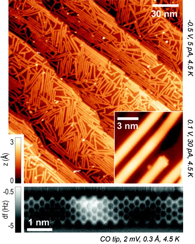
The microscopic ribbons lie criss-crossed on the gold substrate. Empa
Graphene ribbons that are only a few atoms wide, so-called graphene nanoribbons, have special electrical properties that make them promising candidates for the nanoelectronics of the future: While graphene – a one atom thin, honeycomb-shaped carbon layer – is a conductive material, it can become a semiconductor in the form of nanoribbons. This means that it has a sufficiently large energy or band gap in which no electron states can exist: it can be turned on and off – and thus may become a key component of nanotransistors.
The smallest details in the atomic structure of these graphene bands, however, have massive effects on the size of the energy gap and thus on how well-suited nanoribbons are as components of transistors. On the one hand, the gap depends on the width of the graphene ribbons, while on the other hand it depends on the structure of the edges.
Since graphene consists of equilateral carbon hexagons, the border may have a zigzag or a so-called armchair shape, depending on the orientation of the ribbons. While bands with a zigzag edge behave like metals, i.e. they are conductive, they become semiconductors with the armchair edge.
This poses a major challenge for the production of nanoribbons: If the ribbons are cut from a layer of graphene or made by cutting carbon nanotubes, the edges may be irregular and thus the graphene ribbons may not exhibit the desired electrical properties.
Creating a semiconductor with nine atoms
Empa researchers in collaboration with the Max Planck Institute for Polymer Research in Mainz and the University of California at Berkeley have now succeeded in growing ribbons exactly nine atoms wide with a regular armchair edge from precursor molecules.
The specially prepared molecules are evaporated in an ultra-high vacuum for this purpose. After several process steps, they are combined like puzzle pieces on a gold base to form the desired nanoribbons of about one nanometer in width and up to 50 nanometers in length.
These structures, which can only be seen with a scanning tunneling microscope, now have a relatively large and, above all, precisely defined energy gap. This enabled the researchers to go one step further and integrate the graphene ribbons into nanotransistors. Initially, however, the first attempts were not very successful: Measurements showed that the difference in the current flow between the “ON” state (i.e. with applied voltage) and the “OFF” state (without applied voltage) was far too small. The problem was the dielectric layer of silicon oxide, which connects the semiconducting layers to the electrical switch contact. In order to have the desired properties, it needed to be 50 nanometers thick, which in turn influenced the behavior of the electrons.
However, the researchers subsequently succeeded in massively reducing this layer by using hafnium oxide(HfO2) instead of silicon oxide as the dielectric material. The layer is therefore now only 1.5 nanometers thin and the “on”-current is orders of magnitudes higher.
Another problem was the incorporation of graphene ribbons into the transistor. In the future, the ribbons should no longer be located criss-cross on the transistor substrate, but rather aligned exactly along the transistor channel. This would significantly reduce the currently high level of non-functioning nanotransistors.
Media Contact
All latest news from the category: Power and Electrical Engineering
This topic covers issues related to energy generation, conversion, transportation and consumption and how the industry is addressing the challenge of energy efficiency in general.
innovations-report provides in-depth and informative reports and articles on subjects ranging from wind energy, fuel cell technology, solar energy, geothermal energy, petroleum, gas, nuclear engineering, alternative energy and energy efficiency to fusion, hydrogen and superconductor technologies.


Newest articles

Security vulnerability in browser interface
… allows computer access via graphics card. Researchers at Graz University of Technology were successful with three different side-channel attacks on graphics cards via the WebGPU browser interface. The attacks…

A closer look at mechanochemistry
Ferdi Schüth and his team at the Max Planck Institut für Kohlenforschung in Mülheim/Germany have been studying the phenomena of mechanochemistry for several years. But what actually happens at the…

Severe Vulnerabilities Discovered in Software to Protect Internet Routing
A research team from the National Research Center for Applied Cybersecurity ATHENE led by Prof. Dr. Haya Schulmann has uncovered 18 vulnerabilities in crucial software components of Resource Public Key…

