UO-industry collaboration points to improved nanomaterials
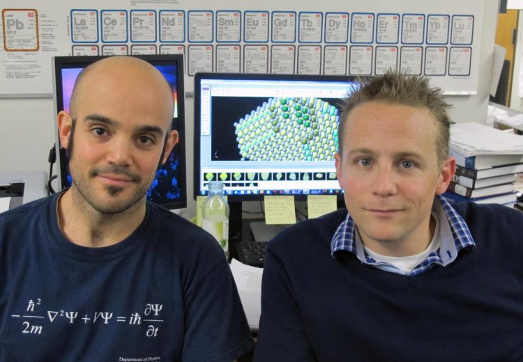
University of Oregon doctoral student Christian Gervasi, left, and Thomas Allen of VoxtelNano led a university-industry collaboration to create atomic-scale maps of the density of states in individual nanocrystals with a specially designed microscope. The maps promise a route to next-generation solar cells. Credit: University of Oregon
A potential path to identify imperfections and improve the quality of nanomaterials for use in next-generation solar cells has emerged from a collaboration of University of Oregon and industry researchers.
To increase light-harvesting efficiency of solar cells beyond silicon's limit of about 29 percent, manufacturers have used layers of chemically synthesized semiconductor nanocrystals. Properties of quantum dots that are produced are manipulated by controlling the synthetic process and surface chemical structure.
This process, however, creates imperfections at the surface-forming trap states that limit device performance. Until recently, improvements in production quality have relied on feedback provided by traditional characterization techniques that probe average properties of large numbers of quantum dots.
“We want to use these materials in real devices, but they are not yet optimized,” said co-author Christian F. Gervasi, a UO doctoral student.
In their study, detailed in the Journal of Physical Chemistry Letters, researchers investigated electronic states of lead sulfide nanocrystals. By using a specially designed scanning tunneling microscope, researchers created atomic-scale maps of the density of states in individual nanocrystals. This allowed them to pinpoint the energies and localization of charge traps associated with defects in the nanocrystal surface structure that are detrimental to electron propagation.
The microscope was designed in the lab of co-author George V. Nazin, a professor in the UO Department of Chemistry and Biochemistry. Its use was described in a previous paper in the same journal, in which Nazin's lab members were able to visualize the internal structures of electronic waves trapped by external electrostatic charges in carbon nanotubes.
“This technology is really cool,” said Peter Palomaki, senior scientist for Voxtel Nanophotonics and co-author on the new paper. “When you really dig down into the science at a very fundamental level, this problem has always been an open-ended question. This paper is just the tip of the iceberg in terms of being able to understand what's going on.”
The insight, he said, should help manufacturers tweak their synthesis of nanocrystals used in a variety of electronic devices. Co-author Thomas Allen, also a senior scientist at Voxtel, agreed. The project began after Allen heard Gervasi and Nazin discussing the microscope's capabilities.
“We wanted to see what the microscope could accomplish, and it turns out that it gives us a lot of information about the trap states and the depths of trap states in our quantum dots,” said Allen, who joined Voxtel after completing the Industrial Internship Program in the UO's Materials Science Institute. “The information will help us fine-tune the ligand chemistry to make better devices for photovoltaics, detectors and sensors.”
The trap states seen by the microscope in this project may explain why nanoparticle-based solar cells have not yet been commercialized, Nazin said.
“Nanoparticles are not always stable. It is a fundamental problem. When you synthesize something at this scale you don't necessarily get the same structure for all of the quantum dots. Working at the atomic scale can produce large variations in the electronic states. Our tool allows us to see these states directly and allow us to provide feedback on the materials.”
Sony Corp. supported the research. Quantum dots were synthesized by VoxtelNanophotonics, a division of Voxtel Inc., which has research space in the UO's Lorry Lokey Laboratories. The microscope, which was described in a recent paper in the journal Review of Scientific Instruments, was built with funding from the National Science Foundation (grant DMR-0960211).
Co-authors with Gervasi, Allen, Palomaki and Nazin are Dmitry A. Kislitsyn and Jason D. Hackley, both doctoral students, and Ryuichiro Maruyama, a courtesy research associate in the Nanoscale Open Research Initiative of the UO's Department of Chemistry and Biochemistry.
Sources: George Nazin, assistant professor of physical chemistry, Department of Chemistry and Biochemistry, 541-346-2017, gnazin@uoregon.edu; Christian Gervasi, doctoral student, 541-346-8150, cgervasi@uoregon.edu; Peter Palomaki, senior scientist, VoxtelNano, a division of Voxtel Inc., 541-346-8131, peterp@voxtel-inc.com; and Thomas Allen, senior scientist, VoxtelNano, a division of Voxtel Inc., 541-346-8131
Note: The University of Oregon is equipped with an on-campus television studio with a point-of-origin Vyvx connection, which provides broadcast-quality video to networks worldwide via fiber optic network. In addition, there is video access to satellite uplink, and audio access to an ISDN codec for broadcast-quality radio interviews.
Previous release: Special UO microscope captures defects in nanotubes: http://uonews.uoregon.edu/archive/news-release/2014/10/special-uo-microscope-captures-defects-nanotubes
New paper abstract: http://pubs.acs.org/doi/abs/10.1021/jz5019465
About Voxtel: http://voxtel-inc.com/about-voxtel/
Nazin faculty page: http://chemistry.uoregon.edu/profile/gnazin/
Nazin Lab: https://wiki.uoregon.edu/display/Nazin/Nazin+Group
Department of Chemistry and Biochemistry: http://chemistry.uoregon.edu/
About the microscope: http://scitation.aip.org/content/aip/journal/rsi/85/10/10.1063/1.4897139
Media Contact
All latest news from the category: Materials Sciences
Materials management deals with the research, development, manufacturing and processing of raw and industrial materials. Key aspects here are biological and medical issues, which play an increasingly important role in this field.
innovations-report offers in-depth articles related to the development and application of materials and the structure and properties of new materials.


Newest articles

Silicon Carbide Innovation Alliance to drive industrial-scale semiconductor work
Known for its ability to withstand extreme environments and high voltages, silicon carbide (SiC) is a semiconducting material made up of silicon and carbon atoms arranged into crystals that is…

New SPECT/CT technique shows impressive biomarker identification
…offers increased access for prostate cancer patients. A novel SPECT/CT acquisition method can accurately detect radiopharmaceutical biodistribution in a convenient manner for prostate cancer patients, opening the door for more…

How 3D printers can give robots a soft touch
Soft skin coverings and touch sensors have emerged as a promising feature for robots that are both safer and more intuitive for human interaction, but they are expensive and difficult…

