Taking Nanolithography Beyond Semiconductors
The process allows scientists to create surfaces with varied chemical functionalities and promises to extend lithography to applications beyond traditional semiconductors. The new technique, which could have a number of practical chemical and biochemical applications, will be described in the 22 December 2006 issue of the journal Advanced Materials by a team led by Paul S. Weiss, distinguished professor of chemistry and physics at Penn State and Mark Horn, associate professor of engineering science and mechanics at Penn State.
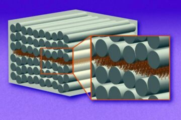
The technique uses self-assembled monolayers (SAM) — chemical films that are one molecule thick — to build a layer on a surface, followed by the addition of a photolithographic resist that protects the covered parts of the film during subsequent processing. The resist acts as a shield during processing, allowing the cleaning and then self-assembly of different chemical functions on the unprotected parts of the surface. “Other chemical patterning processes on surfaces suffer from cross-reactions and dissolution at their boundaries,” says Weiss. “In our process, the resist provides a barrier and prevents interactions between the molecules already on the surface and the chemistry being done elsewhere. The resist is placed on top of the pattern by standard photolithographic techniques. After the resist is placed, molecules are removed from the exposed areas of the surface. Subsequent placement of a different SAM on the exposed surface creates a pattern of different films, with different functionalities.
Because the resist protects everything it covers, the layer under it does not have to be a single functionality. As a result, a series of pattern/protect/remove/repattern cycles can be applied, allowing complex patterns of functional monolayers on the surface of the substrate. “It allows us to work stepwise across a surface, building complex patterns,” says Weiss. “We have demonstrated patterns at the micrometer scale and have the potential to go down to nanometer-scale patterns.” While the two processes used by the team — molecular self-assembly and photolithography — are individually well-developed, the team's innovation is the successful combination of the techniques to build well-defined surfaces.
Chemical functionalities are distributed across the surface in high-quality layers as a result of the self-assembly process and in high-resolution patterns due to the use of the specialized resists. Different chemical functionalities can be used to detect or to separate a variety of species from a mixture. “The product of the process can be used to create a multiplexed, patterned, capture surface,” says Weiss. “We could expose the entire surface to one mixture and capture different parts of the mixture in each region.”
The work was a collaborative effort between the Weiss group, specializing in surface chemistry, and the Horn group, specializing in nanolithography. In addition to Weiss and Horn, the Penn State research team included graduate students Mary E. Anderson (now graduated), Charan Srinivasan, and J. Nathan Hohman, as well as undergraduate researcher Erin Carter. The work was performed as a part of both the National Science Foundation supported Center for Nanoscale Science and Penn State's node of the National Nanofabrication Infrastructure Network.
Media Contact
More Information:
http://www.psu.eduAll latest news from the category: Materials Sciences
Materials management deals with the research, development, manufacturing and processing of raw and industrial materials. Key aspects here are biological and medical issues, which play an increasingly important role in this field.
innovations-report offers in-depth articles related to the development and application of materials and the structure and properties of new materials.


Newest articles
“Nanostitches” enable lighter and tougher composite materials
In research that may lead to next-generation airplanes and spacecraft, MIT engineers used carbon nanotubes to prevent cracking in multilayered composites. To save on fuel and reduce aircraft emissions, engineers…
Trash to treasure
Researchers turn metal waste into catalyst for hydrogen. Scientists have found a way to transform metal waste into a highly efficient catalyst to make hydrogen from water, a discovery that…
Real-time detection of infectious disease viruses
… by searching for molecular fingerprinting. A research team consisting of Professor Kyoung-Duck Park and Taeyoung Moon and Huitae Joo, PhD candidates, from the Department of Physics at Pohang University…

