Powerful New Technique Simultaneously Determines Nanomaterials' Chemical Makeup, Topography

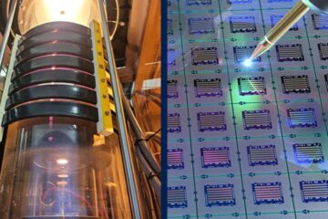
The technique combines synchrotron X-rays (SX) and scanning tunneling microscopy (STM). In experiments, the researchers used SX as a probe and a nanofabricated smart tip of a STM as a detector.
Using this technique, researchers detected the chemical fingerprint of individual nickel clusters on a copper surface at a two-nanometer (nm) lateral resolution, and at the ultimate single atom height sensitivity. By varying the photon energy, the researchers used the difference in photoabsorption cross sections for nickel and the copper substrate to chemically image a single-nickel nanocluster – thus opening the door to new opportunities for chemical imaging of nanoscale materials. Until now, a spatial limit of about only 10-nm was attainable, and the researchers would simultaneously sample a large sample area. The researchers have improved the spatial resolution to 2 nm.
“Imaging with direct chemical sensitivity has been a long-standing goal since scanning tunneling microscopes were developed during the 1980s,” said Volker Rose, a physicist in the X-ray Science Division. “It was very exciting when we obtained elemental contrast of a material at just one atomic layer height”.
“This is a marriage between two of the most powerful instruments of materials science,” said Saw-Wai Hla, electronic and magnetic materials and devices group leader in Argonne's Nanoscience & Technology Division. “We now have an instrument that can perform the functions of STM and X-rays in a single setting, and therefore it has a great potential to revolutionize the materials characterization.”
To conduct the experiment, researchers used the Center for Nanoscale Materials’ (CNM) beamline 26-ID at the Advanced Photon Source (APS), which is equipped with two collinear undulator devices that serve as the X-ray source and a double-crystal monochromater that selects the photon energy. The X-rays were passed through a beam chopper to quickly turn the beam on and off and then illuminate the tip/sample junction in the SX-STM. This enabled the very sensitive lock-in detection of the X-ray induced currents.
The experiment was conducted at room temperature, which is well suited for the needs of most physical, chemical, biological and nanomaterial applications. The team anticipates that even higher spatial resolution may become possible with a new instrument currently under development.
“The next step will be to extend the new technique to low temperatures,” notes Rose. “Our measurements indicate that atomic resolution may be achievable at 5 K (about negative 450 F).”
This research was funded by the DOE Office of Science Early Career Research Program. The APS and CNM are DOE Office of Science User Facilities located at Argonne.
Nozomi Shirato, Marvin Cummings and Benjamin Stripe, postdoctoral appointees at Argonne, and Heath Kersell and Yang Li, graduate students in physics at Ohio University, helped to conduct the experiments. Saw-Wai Hla and Volker Rose, of Argonne, designed the experiment and Daniel Rosenmann, of Argonne, made the smart tip. Curt Preissner, of Argonne’s APS Engineering Support Division, provided engineering support, and Jon Hiller, formerly of CNM’s Electron Microscopy Center group, helped to make the smart tip.
To view the publication “Elemental Fingerprinting of Materials with Sensitivity at the Atomic Limit” in NanoLetters, visit the ACS publications website.
To learn more about the project, visit the SXSPM website.
Argonne National Laboratory seeks solutions to pressing national problems in science and technology. The nation's first national laboratory, Argonne conducts leading-edge basic and applied scientific research in virtually every scientific discipline. Argonne researchers work closely with researchers from hundreds of companies, universities, and federal, state and municipal agencies to help them solve their specific problems, advance America's scientific leadership and prepare the nation for a better future. With employees from more than 60 nations. Argonne is supported by the Office of Science of the U.S. Department of Energy. The Office of Science is the single largest supporter of basic research in the physical sciences in the United States, and is working to address some of the most pressing challenges of our time. For more information, please visit science.energy.gov.”
Contact Information
Tona Kunz
Communication Lead
tkunz@anl.gov
Phone: (630) 252-5560
Media Contact
More Information:
http://www.anl.gov/All latest news from the category: Materials Sciences
Materials management deals with the research, development, manufacturing and processing of raw and industrial materials. Key aspects here are biological and medical issues, which play an increasingly important role in this field.
innovations-report offers in-depth articles related to the development and application of materials and the structure and properties of new materials.
Newest articles

Silicon Carbide Innovation Alliance to drive industrial-scale semiconductor work
Known for its ability to withstand extreme environments and high voltages, silicon carbide (SiC) is a semiconducting material made up of silicon and carbon atoms arranged into crystals that is…

New SPECT/CT technique shows impressive biomarker identification
…offers increased access for prostate cancer patients. A novel SPECT/CT acquisition method can accurately detect radiopharmaceutical biodistribution in a convenient manner for prostate cancer patients, opening the door for more…

How 3D printers can give robots a soft touch
Soft skin coverings and touch sensors have emerged as a promising feature for robots that are both safer and more intuitive for human interaction, but they are expensive and difficult…


