Plasmonics: Minimizing loss by thinning and smoothing
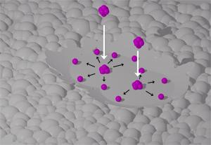
The smoothing effect of a gas cluster ion beam (purple) on a rough surface (gray). Copyright : 2014 A*STAR Institute of Materials Research and Engineering
Plasmonic devices — such as superlenses, hyperlenses and plasmonic waveguides — have exciting potential for research and commercial applications because they permit optical lithography, imaging and waveguiding to be performed at resolutions below the diffraction limit of light.
These devices often require low-loss ultrathin metal films, which are difficult to fabricate using current deposition techniques. Researchers have investigated processes such as seed layer deposition and thermal annealing to reduce the surface roughness and grain-boundary density of these films. To date, however, these processes have not been hugely successful.
Now, Ee Jin Teo and colleagues at the A*STAR Institute of Materials Research and Engineering, Singapore, the University of Hyogo, Japan, and the National University of Singapore have used gas cluster ion beam (GCIB) processing to smooth ultrathin metal films and thereby enhance their properties(1).
A GCIB consists of thousands of gas molecules that are weakly bound by van der Waals forces. Such a beam is able to smooth out surface irregularities and reduce film thickness with nanometer precision. This processing significantly enhances surface plasmon resonance and propagation, and enables the fabrication of ultrathin films with extremely low electrical resistivity and optical loss.
Unlike monomer ion beams used in conventional ion-beam milling and plasma etching, a cluster of nitrogen gas molecules with an energy of 20 kiloelectron volts impinging on a silver film can deliver a high energy density to a relatively small volume: yet the cluster penetrates to a depth of only a few nanometers.
The impact of the beam on the film causes silver atoms in surface peaks to scatter sideways towards valleys, voids and grain boundaries. As well as producing a smoother surface, this processing triples the grain width through the redeposition of atoms at grain boundaries.
The team’s GCIB treatment resulted in up to a four-fold improvement in the electrical and optical properties of films of a thickness of 12 nanometers. “The unique characteristics of GCIB irradiation meant that in a single irradiation step we could reduce scattering losses due to surface roughness, grain boundaries and voids,” notes Teo.
The research team also used the technique to smooth the top surface and sidewalls of lithographically patterned silver-stripe waveguides, increasing the propagation lengths of surface plasmons in these waveguides.
“In the future, we intend to use this technique to improve the colour purity of plasmonic color filters or reflectors, and also to increase the patterned area of superlens nanolithography,” says Teo. “Such developments will bring plasmonic research a step closer to commercialization.”
Reference
1. Teo, E. J., Toyoda, N., Yang, C., Wang, B., Zhang, N. et al. Sub-30 nm thick plasmonic films and structures with ultralow loss. Nanoscale 6, 3243–3249 (2014).
Associated links
Media Contact
More Information:
http://www.researchsea.comAll latest news from the category: Materials Sciences
Materials management deals with the research, development, manufacturing and processing of raw and industrial materials. Key aspects here are biological and medical issues, which play an increasingly important role in this field.
innovations-report offers in-depth articles related to the development and application of materials and the structure and properties of new materials.


Newest articles

Superradiant atoms could push the boundaries of how precisely time can be measured
Superradiant atoms can help us measure time more precisely than ever. In a new study, researchers from the University of Copenhagen present a new method for measuring the time interval,…

Ion thermoelectric conversion devices for near room temperature
The electrode sheet of the thermoelectric device consists of ionic hydrogel, which is sandwiched between the electrodes to form, and the Prussian blue on the electrode undergoes a redox reaction…

Zap Energy achieves 37-million-degree temperatures in a compact device
New publication reports record electron temperatures for a small-scale, sheared-flow-stabilized Z-pinch fusion device. In the nine decades since humans first produced fusion reactions, only a few fusion technologies have demonstrated…

