New Path to Flex and Stretch Electronics
Imprinting electronic circuitry on backplanes that are both flexible and stretchable promises to revolutionize a number of industries and make “smart devices” nearly ubiquitous.
Among the applications that have been envisioned are electronic pads that could be folded away like paper, coatings that could monitor surfaces for cracks and other structural failures, medical bandages that could treat infections and food packaging that could detect spoilage. From solar cells to pacemakers to clothing, the list of smart applications for so-called “plastic electronics” is both flexible and stretchable. First, however, suitable backplanes must be mass-produced in a cost-effective way.
Researchers with the U.S. Department of Energy (DOE)’s Lawrence Berkeley National Laboratory (Berkeley Lab) have developed a promising new inexpensive technique for fabricating large-scale flexible and stretchable backplanes using semiconductor-enriched carbon nanotube solutions that yield networks of thin film transistors with superb electrical properties, including a charge carrier mobility that is dramatically higher than that of organic counterparts. To demonstrate the utility of their carbon nanotube backplanes, the researchers constructed an artificial electronic skin (e-skin) capable of detecting and responding to touch.
“With our solution-based processing technology, we have produced mechanically flexible and stretchable active-matrix backplanes, based on fully passivated and highly uniform arrays of thin film transistors made from single walled carbon nanotubes that evenly cover areas of approximately 56 square centimeters,” says Ali Javey, a faculty scientist in Berkeley Lab’s Materials Sciences Division and a professor of electrical engineering and computer science at the University of California (UC) Berkeley. “This technology, in combination with inkjet printing of metal contacts, should provide lithography-free fabrication of low-cost flexible and stretchable electronics in the future.”
Javey is the corresponding author of a paper in the journal NanoLetters that describes this work titled “Carbon Nanotube Active-Matrix Backplanes for Conformal Electronics and Sensors.” Co-authoring this paper were Toshitake Takahashi, Kuniharu Takei, Andrew Gillies and Ronald Fearing.
With the demand for plastic electronics so high, research and development in this area has been intense over the past decade. Single walled carbon nanotubes (SWNTs) have emerged as one of the top contending semiconductor materials for plastic electronics, primarily because they feature high mobility for electrons – a measure of how fast a semiconductor conducts electricity. However, SWNTs can take the form of either a semiconductor or a metal and a typical SWNT solution consists of two-thirds semiconducting and one-third metallic tubes. This mix yields nanotube networks that exhibit low on/off current ratios, which poses a major problem for electronic applications as lead author of the NanoLetters paper Takahashi explains.
“An on/off current ratio as high as possible is essential for reducing the interruption from pixels in an off-state,” he says. “For example, with our e-skin device, when we are pressure mapping, we want to get the signal only from the on-state pixel on which pressure is applied. In other words, we want to minimize the current as small as possible from the other pixels which are supposed to be turned off. For this we need a high on/off current ratio.”
To make their backplanes, Javey, Takahashi and their co-authors used a SWNT solution enriched to be 99-percent semiconductor tubes. This highly purified solution provided the researchers with a high on/off ratio (approximately 100) for their backplanes. Working with a thin substrate of polymide, a high-strength polymer with superior flexibility, they laser-cut a honeycomb pattern of hexagonal holes that made the substrate stretchable as well. The holes were cut with a fixed pitch of 3.3 millimeters and a varied hole-side length that ranged from 1.0 to 1.85 millimeters.
“The degree to which the substrate could be stretched increased from 0 to 60-percent as the side length of the hexagonal holes increased to 1.85 mm,” Takahashi says. “In the future, the degrees of stretchability and directionality should be tunable by either changing the hole size or optimizing the mesh design.”
Backplanes were completed with the deposition on the substrates of layers of silicon and aluminum oxides followed by the semiconductor-enriched SWNTs. The resulting SWNT thin film transistor backplanes were used to create e-skin for spatial pressure mapping. The e-skin consisted of an array of 96 sensor pixels, measuring 24 square centimeters in area, with each pixel being actively controlled by a single thin film transistor. To demonstrate pressure mapping, an L-shaped weight was placed on top of the e-skin sensor array with the normal pressure of approximately 15 kilo Pascals (313 pounds per square foot).
“In the linear operation regime, the measured sensor sensitivity reflected a threefold improvement compared with previous nanowire-based e-skin sensors reported last year by our group,” Takahashi says. “This improved sensitivity was a result of the improved device performance of the SWNT backplanes. In the future we should be able to expand our backplane technology by adding various sensor and/or other active device components to enable multifunctional artificial skins. In addition, the SWNT backplane could be used for flexible displays.”
This research was supported in part by the DOE Office of Science and in part by the National Science Foundation.
Lawrence Berkeley National Laboratory addresses the world’s most urgent scientific challenges by advancing sustainable energy, protecting human health, creating new materials, and revealing the origin and fate of the universe. Founded in 1931, Berkeley Lab’s scientific expertise has been recognized with 12 Nobel prizes. The University of California manages Berkeley Lab for the U.S. Department of Energy’s Office of Science. For more, visit www.lbl.gov.
Additional Information
For more information about the research of Ali Javey, visit the Website at http://nano.eecs.berkeley.edu/
Media Contact
All latest news from the category: Materials Sciences
Materials management deals with the research, development, manufacturing and processing of raw and industrial materials. Key aspects here are biological and medical issues, which play an increasingly important role in this field.
innovations-report offers in-depth articles related to the development and application of materials and the structure and properties of new materials.


Newest articles
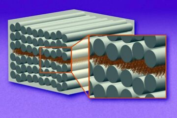
“Nanostitches” enable lighter and tougher composite materials
In research that may lead to next-generation airplanes and spacecraft, MIT engineers used carbon nanotubes to prevent cracking in multilayered composites. To save on fuel and reduce aircraft emissions, engineers…
Trash to treasure
Researchers turn metal waste into catalyst for hydrogen. Scientists have found a way to transform metal waste into a highly efficient catalyst to make hydrogen from water, a discovery that…

Real-time detection of infectious disease viruses
… by searching for molecular fingerprinting. A research team consisting of Professor Kyoung-Duck Park and Taeyoung Moon and Huitae Joo, PhD candidates, from the Department of Physics at Pohang University…

