ORNL research uncovers path to defect-free thin films
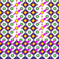
A schematic of a regular atomic array of ferromagnetic nano-domains formed due to an unconventional strain relaxation.<br>
The finding, published in Nano Letters, could change the conventional wisdom that accommodating the strain inherent during the formation of epitaxial thin films necessarily involves structural defects, said Lee, a member of the Department of Energy lab's Materials Science and Technology Division.
Instead, the researchers found that some materials, in this case cobaltite, form structurally well ordered atomic patterns that can change their magnetic properties and effectively minimize the size mismatch with the crystalline substrate.
Epitaxial thin films, used in nanotechnology and semiconductor fabrication, are created by growing a crystal layer of one material on another in such a way that the crystalline structures align. The challenge is to grow the film coherently with minimal defects, which can have a catastrophic effect on a material's performance.
“We discovered properties that were not readily apparent in crystal, or bulk, form, but in thin-film form we were able to clearly see the atomically ordered lattice structure of lanthanum cobaltite,” Lee said. “With this knowledge, we hope to be able to tailor the physical properties of a material for many information and energy technologies.”
The researchers studied the material in different strain states using scanning transmission electron microscopy complemented by X-ray and optical spectroscopy. Using these instruments, the scientists could see unconventional strain relaxation behavior that produced stripe-like lattice patterns. The result is a material with useful magnetic properties and highly suitable for sensors and ionic conductors used in, for example, batteries.
This discovery and the ability to engineer the structure of materials could lead to advanced cathode materials in solid oxide fuel cells and batteries that can be charged much faster.
“Since cobaltites are promising candidates for magnetic sensors, ionic conductors and surface catalysts, this discovery provides a new understanding that can be used for artificial tuning of magnetism and ionic activities,” Lee said.
Contributing to the paper were ORNL's Woo Seok Choi and Hyoungjeen Jeen and authors from Seoul National University, the University of British Columbia, IFW Dresden's Leibniz Institute for Solid Sate and Materials Research, Max Planck-UBC Centre for Quantum Materials, Max Planck Institute for Solid State Research and the University of Saskatchewan.
The paper, titled “Strain-Induced Spin States in Atomically Ordered Cobaltites,” is available at http://pubs.acs.org/doi/abs/10.1021/nl302562f. Funding for this work was provided primarily by the U.S. Department of Energy's Office of Science, Basic Energy Sciences. Optical measurements were performed in part at the Center for Nanophase Materials Sciences, a DOE-Basic Energy Sciences user facility.
This work was supported by the Center for Nanophase Materials Sciences at ORNL. CNMS is one of the five DOE Nanoscale Science Research Centers supported by the DOE Office of Science, premier national user facilities for interdisciplinary research at the nanoscale. Together the NSRCs comprise a suite of complementary facilities that provide researchers with state-of-the-art capabilities to fabricate, process, characterize and model nanoscale materials, and constitute the largest infrastructure investment of the National Nanotechnology Initiative. The NSRCs are located at DOE's Argonne, Brookhaven, Lawrence Berkeley, Oak Ridge and Sandia and Los Alamos national laboratories. For more information about the DOE NSRCs, please visit http://science.energy.gov/bes/suf/user-facilities/nanoscale-science-research-centers/.
UT-Battelle manages ORNL for the Office of Science. The Office of Science is the single largest supporter of basic research in the physical sciences in the United States and is working to address some of the most pressing challenges of our time. For more information, please visit http://science.energy.gov/
Media Contact
All latest news from the category: Materials Sciences
Materials management deals with the research, development, manufacturing and processing of raw and industrial materials. Key aspects here are biological and medical issues, which play an increasingly important role in this field.
innovations-report offers in-depth articles related to the development and application of materials and the structure and properties of new materials.


Newest articles

Silicon Carbide Innovation Alliance to drive industrial-scale semiconductor work
Known for its ability to withstand extreme environments and high voltages, silicon carbide (SiC) is a semiconducting material made up of silicon and carbon atoms arranged into crystals that is…

New SPECT/CT technique shows impressive biomarker identification
…offers increased access for prostate cancer patients. A novel SPECT/CT acquisition method can accurately detect radiopharmaceutical biodistribution in a convenient manner for prostate cancer patients, opening the door for more…

How 3D printers can give robots a soft touch
Soft skin coverings and touch sensors have emerged as a promising feature for robots that are both safer and more intuitive for human interaction, but they are expensive and difficult…

