Next generation of watch springs
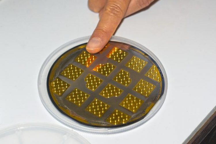
The watch springs are electroplated on a gold plated silicon wafer, coated with a light-sensitive paint. Empa
Applied research is not always initiated by industry – but oftentimes it yields results that can swiftly be implemented by companies. A prime example can be seen on the Empa campus in Thun: Tiny watch springs are on display at the Laboratory for Mechanics of Materials and Nanostructures.
These springs – the beating heart of every mechanical clock – are not your usual components. They are not made of the famous Nivarox wires, but rather deposited electrically – or, rather, electrochemically – in the desired form from a cold, aqueous saline solution.
By now, the production in the Empa lab has outgrown the first pilot tests. On a regular basis the electroplated springs are delivered to the R&D department at a major Swiss watchmaker, where they are fitted in prototype watch mechanisms. The watches run. However, there is still work to do on their accuracy and long-term stability.
Only a few years ago, Empa had to rely on partners to take care of certain process steps. Meanwhile, the knowhow for the entire production process is pooled in Michler’s lab. Laetitia Philippe, who oversees the production of the springs, explains the production steps. The base material is a silicon wafer like the ones used to produce computer chips and solar cells.
This wafer is initially coated with a conductive gold layer and, later on, a thin layer of light-sensitive paint. The shape of the spring is then projected onto it and the illuminated parts of the paint are etched out. Now the desired metallic alloy can be electroplated onto the conductive gold base.
As Philippe knows only too well, this crucial step in the process is tricky. “We need a good swirl in the galvanic bath, the right temperature, some organic additives and a current at just the right strength and – if it’s alternating current – in the right form.”
Eventually, the goal is to dissolve the springs out of the galvanic mold. Initially, the researchers use a light microscope to check whether the spring molds are filled correctly with metal. Then the top side of the mold is fine-polished to ensure all springs are of a defined thickness; the result is verified via X-ray fluorescence analysis.
Finally, the paint is removed with an oxygen plasma, the silicon wafer etched away using a strong alkaline solution and the gold coating dissolved. The remaining springs then need to go into a special washing machine for a few hours to remove any ridges and protruding metal remnants. These flawless springs then go into the watch lab for prototype production.
A by-product of research
For the researchers at Empa, however, this kind of prototype production is only one aspect of their scientific work. “Our goal is certainly not to compete with suppliers in the watch industry,” says Michler. “At Empa, we are mainly interested in the process of miniaturization itself.” Michler’s team studies the mechanical properties of the tiny parts with minuscule stamps and needles. After all, the properties of materials change if we build tiny parts: Ductile metals become harder; brittle ceramics, on the other hand, become ductile with very small component sizes.
“The prerequisite for any examination, however, is that we are able to produce the objects we are interested in based on defined criteria,” explains the Empa researcher. Thus, Michler’s team not only strives to master one single process step, but also keep a grip on the quality of the entire process chain. “Some process steps are closely intertwined,” says Michler. “If we change one parameter, such as the geometry of the electroplating molds or the composition of the alloy, we usually have to adjust the preceding and subsequent steps, too. We want to understand these connections and the effects of miniaturization in every aspect.”
Additive manufacturing in 3D
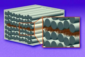
Besides two-dimensional structures, the researchers in Thun have already made progress in the production of 3D structures – also with the aid of electroplating. The required molds are not produced by illuminating layers of paint on silicon wafers, but rather via what is known as two-photon polymerization. This involves emitting a laser beam in a container with a special liquid plastic precursor. In the focal point of the beam, the liquid polymerizes and solidifies.
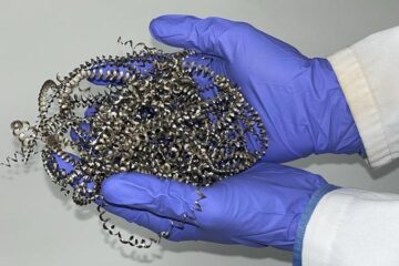
The Empa team succeeded in making delicate structures and electroplating them with a nickel boron coating. In strength tests, these metallized structures exhibited much more stability than the raw polymer scaffold. Meanwhile, the researchers have also managed to produce bridges and columns made of solid nickel that are merely a few micrometers in size. Stress tests reveal how the nickel alloys behave in these dimensions.
“We are already able to make such structures with a nice regularity and in a replicable manner,” says Laetitia Philippe. “We have taken a major step forward on the road towards micromechanics made of electroplated components.” In the not too distant future, these components might permit clock mechanisms with particularly fine mechanical complications.
Dr. Johann Michler
Mechanics of Materials and Nanostructures
Phone +41 58 765 62 05
Johann.Michler@empa.ch
P Schürch, L Pethö, J Schwiedrzik, J Michler, L Philippe; Additive Manufacturing through Galvanoforming of 3D Nickel Microarchitectures: Simulation‐Assisted Synthesis; Advanced Material Technologies (2018); doi: 10.1002/admt.201800274
https://onlinelibrary.wiley.com/doi/abs/10.1002/admt.201800274
Media Contact
All latest news from the category: Materials Sciences
Materials management deals with the research, development, manufacturing and processing of raw and industrial materials. Key aspects here are biological and medical issues, which play an increasingly important role in this field.
innovations-report offers in-depth articles related to the development and application of materials and the structure and properties of new materials.


Newest articles
“Nanostitches” enable lighter and tougher composite materials
In research that may lead to next-generation airplanes and spacecraft, MIT engineers used carbon nanotubes to prevent cracking in multilayered composites. To save on fuel and reduce aircraft emissions, engineers…
Trash to treasure
Researchers turn metal waste into catalyst for hydrogen. Scientists have found a way to transform metal waste into a highly efficient catalyst to make hydrogen from water, a discovery that…

Real-time detection of infectious disease viruses
… by searching for molecular fingerprinting. A research team consisting of Professor Kyoung-Duck Park and Taeyoung Moon and Huitae Joo, PhD candidates, from the Department of Physics at Pohang University…

