Nanoparticles: Making gold economical for sensing
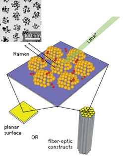
Schematic of the nanocluster SERS substrate in planar chip and fiber-optic configurations. The dome shape of the gold nanoclusters reflects the shape of the hemispherical polymer nanostructures on the underlying surface. The red/green clusters represent the molecules being analyzed. The arrays are densely packed and regularly spaced (inset: electron micrograph of the arrays). Reproduced, with permission, from Ref. 1 © 2012 American Chemical Society (inset); © 2012 A*STAR Institute of Materials Research and Engineering (main image)<br>
Cancer, food pathogens and biosecurity threats can all be detected using a sensing technique called surface enhanced Raman spectroscopy (SERS). To meet ever-increasing demands in sensitivity, however, signals from molecules of these agents require massive enhancement, and current SERS sensors require optimization. An A*STAR-led research team recently fabricated a remarkably regular array of closely packed gold nanoparticle clusters that will improve SERS sensors.
So-called ‘Raman scattering’ occurs when molecules scatter at wavelengths not present in the incident light. These molecules can be detected with SERS sensors by bringing them into contact with a nanostructured metal surface, illuminated by a laser at a particular wavelength. An ideal sensor surface should have: dense packing of metal nanostructures, commonly gold or silver, to intensify Raman scattering; a regular arrangement to produce repeatable signal levels; economical construction; and robustness to sustain sensing performance over time.
Few of the many existing approaches succeed in all categories. However, Fung Ling Yap and Sivashankar Krishnamoorthy at the A*STAR Institute of Materials Research and Engineering, Singapore, and co-workers produced closely packed nanocluster arrays of gold that incorporate the most desirable aspects for fabrication and sensing. In addition to flat surfaces, they also succeeded in coating fiber-optic tips with similarly dense nanocluster arrays (see image), which is a particularly promising development for remote-sensing applications, such as hazardous waste monitoring.
The researchers self-assembled their arrays by using surfaces coated with self-formed polymer nanoparticles, to which smaller gold nanoparticles spontaneously attached to form clusters. “It was surprising to reliably attain feature separations of less than 10 nanometers, at high yield, across macroscopic areas using simple processes such as coating and adsorption,” notes Krishnamoorthy.
By varying the size and density of the polymer features, Krishnamoorthy, Yap and co-workers tuned the cluster size and density to maximize SERS enhancements. Their technique is also efficient: less than 10 milligrams of the polymer and 100 milligrams of gold nanoparticles are needed to coat an entire 100 millimeter diameter wafer, or approximately 200 fiber tips. Both the polymer and the nanoparticles can be mass-produced at low cost. By virtue of being entirely ‘self-assembled’, the technique does not require specialized equipment or a custom-built clean room, so it is well suited to low-cost commercial implementation.
“We have filed patent applications for the work in Singapore, the USA and China,” says Krishnamoorthy. “The arrays are close to commercial exploitation as disposable sensor chips for use in portable SERS sensors, in collaboration with industry.”
The A*STAR-affiliated researchers contributing to this research are from the Institute of Materials Research and Engineering
References
Yap, F. L., Thoniyot, P., Krishnan, S. & Krishnamoorthy, S. Nanoparticle cluster arrays for high-performance SERS through directed self-assembly on flat substrates and on optical fibers. ACS Nano 6, 2056–2070 (2012).
Media Contact
All latest news from the category: Materials Sciences
Materials management deals with the research, development, manufacturing and processing of raw and industrial materials. Key aspects here are biological and medical issues, which play an increasingly important role in this field.
innovations-report offers in-depth articles related to the development and application of materials and the structure and properties of new materials.


Newest articles

Properties of new materials for microchips
… can now be measured well. Reseachers of Delft University of Technology demonstrated measuring performance properties of ultrathin silicon membranes. Making ever smaller and more powerful chips requires new ultrathin…

Floating solar’s potential
… to support sustainable development by addressing climate, water, and energy goals holistically. A new study published this week in Nature Energy raises the potential for floating solar photovoltaics (FPV)…

Skyrmions move at record speeds
… a step towards the computing of the future. An international research team led by scientists from the CNRS1 has discovered that the magnetic nanobubbles2 known as skyrmions can be…

