Multitasking monolayers
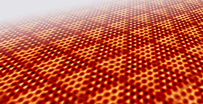
This is an illustration of the triangular pattern formed by the two-dimensional material chalcogenide that allows the creation of dual-function devices. Credit: Yu-Yang Zhang, Chinese Academy of Sciences
That is the result of a new process that naturally produces patterned monolayers that can act as a base for creating a wide variety of novel materials with dual optical, magnetic, catalytic or sensing capabilities.
“Patterned materials open up the possibility of having two functionalities in a single material, such as catalyzing a chemical reaction while simultaneously serving as a sensor for a second set of molecules,” said Sokrates Pantelides, William and Nancy McMinn Professor of Physics at Vanderbilt University, who coordinated the research with Professor Hong-Jun Gao at the Institute of Physics of the Chinese Academy of Sciences in Beijing. “Of course, you can do such a thing by using two materials side by side, but patterned materials offer a whole range of new options for device designers.”
Their achievement is described in a paper titled “Intrinsically patterned two-dimensional materials for selective adsorption of molecules and nanoclusters” published Jun. 12 in the journal Nature Materials.
In electronics, two dimensional (2D) materials are a hot topic because of their many potential applications. Graphene, which consists of a single sheet of carbon atoms, has received the most attention, but it has proven very difficult to tune its chemical and electrical properties. As a result, chalcogenides (materials that contain sulfur, selenium or tellurium, which are known for their widely varied optical, electrical and thermal properties) are now the focus of worldwide research because some of them naturally form monolayers that can serve as blank slates that are readily tailored for specific applications.
Now, Pantelides and his collaborators have shown that monolayers formed by two chalcogenides (platinum-selenium and copper-selenium) naturally combine with nanoscale precision into alternating triangles with different phases: metallic and semiconductor. Because each phase has different electrical and chemical properties, two different types of molecules can bond to its surface, allowing it to perform two functions simultaneously.
“In general, 2D materials are 'functionalized' for specific applications by adsorbing different species of atoms or molecules on them or by embedding impurities in their otherwise perfect crystalline structure in the same way that semiconductors such as silicon are functionalized by doping with impurities, which enables the fabrication of electronic devices, such as the 'chips' that drive computers,” Pantelides explained. “Our new paper extends the realm of 2D materials by one important step. It demonstrates a way to fabricate 2D materials that allows the two phases of the material to be functionalized independently.”
The experiments were conducted in Gao's laboratory in Beijing and theoretical calculations were performed at Vanderbilt, the U.S Department of Energy's National Energy Research Scientific Computing Center and the University of the Chinese Academy of Sciences.
The research was funded by U.S. Department of Energy grants DE-FG02-09ER46554, National Key Research and Development Projects of China (2016YFA0202300), the National Basic Research Program of China (2013CBA01600) and the National Natural Science Foundation of China (61390501, 51572290, 61306015 and 61471337, 51325204) and the Chinese Academy of Sciences (1731300500015, XDB07030100.)
Media Contact
All latest news from the category: Materials Sciences
Materials management deals with the research, development, manufacturing and processing of raw and industrial materials. Key aspects here are biological and medical issues, which play an increasingly important role in this field.
innovations-report offers in-depth articles related to the development and application of materials and the structure and properties of new materials.


Newest articles
Combatting disruptive ‘noise’ in quantum communication
In a significant milestone for quantum communication technology, an experiment has demonstrated how networks can be leveraged to combat disruptive ‘noise’ in quantum communications. The international effort led by researchers…

Stretchable quantum dot display
Intrinsically stretchable quantum dot-based light-emitting diodes achieved record-breaking performance. A team of South Korean scientists led by Professor KIM Dae-Hyeong of the Center for Nanoparticle Research within the Institute for…

Internet can achieve quantum speed with light saved as sound
Researchers at the University of Copenhagen’s Niels Bohr Institute have developed a new way to create quantum memory: A small drum can store data sent with light in its sonic…

