Lawrence Livermore researchers develop efficient method to produce nanoporous metals
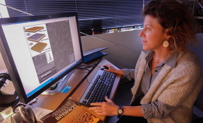
Tiziana Bond, an LLNL engineer who is a member of the joint research team, helped developed a cost-effective and more efficient way to manufacture nanoporous metals over many scales, from nanoscale to macroscale, which is visible to the naked eye. Photo by Julie Russell/LLNL
They posses a high surface area for better electron transfer, which can lead to the improved performance of an electrode in an electric double capacitor or battery. Nanoporous metals offer an increased number of available sites for the adsorption of analytes, a highly desirable feature for sensors.
Lawrence Livermore National Laboratory (LLNL) and the Swiss Federal Institute of Technology (ETH) researchers have developed a cost-effective and more efficient way to manufacture nanoporous metals over many scales, from nanoscale to macroscale, which is visible to the naked eye.
The process begins with a four-inch silicon wafer. A coating of metal is added and sputtered across the wafer. Gold, silver and aluminum were used for this research project. However, the manufacturing process is not limited to these metals.
Next, a mixture of two polymers is added to the metal substrate to create patterns, a process known as diblock copolymer lithography (BCP). The pattern is transformed in a single polymer mask with nanometer-size features. Last, a technique known as anisotropic ion beam milling (IBM) is used to etch through the mask to make an array of holes, creating the nanoporous metal.
During the fabrication process, the roughness of the metal is continuously examined to ensure that the finished product has good porosity, which is key to creating the unique properties that make nanoporous materials work. The rougher the metal is, the less evenly porous it becomes.
“During fabrication, our team achieved 92 percent pore coverage with 99 percent uniformity over a 4-in silicon wafer, which means the metal was smooth and evenly porous,” said Tiziana Bond, an LLNL engineer who is a member of the joint research team.
The team has defined a metric — based on a parametrized correlation between BCP pore coverage and metal surface roughness — by which the fabrication of nanoporous metals should be stopped when uneven porosity is the known outcome, saving processing time and costs.
“The real breakthrough is that we created a new technique to manufacture nanoporous metals that is cheap and can be done over many scales avoiding the lift-off technique to remove metals, with real-time quality control,” Bond said. “These metals open the application space to areas such as energy harvesting, sensing and electrochemical studies.”
The lift-off technique is a method of patterning target materials on the surface of a substrate by using a sacrificial material. One of the biggest problems with this technique is that the metal layer cannot be peeled off uniformly (or at all) at the nanoscale.
Advanced Materials Interfaces
The research team’s findings were reported in an article titled “Manufacturing over many scales: High fidelity macroscale coverage of nanoporous metal arrays via lift-off-free nanofrabication.” It was the cover story in a recent issue of Advanced Materials Interfaces.
Other applications of nanoporous metals include supporting the development of new metamaterials (engineered materials) for radiation-enhanced filtering and manipulation, including deep ultraviolet light. These applications are possible because nanoporous materials facilitate anomalous enhancement of transmitted (or reflected) light through the tunneling of surface plasmons, a feature widely usable by light-emitting devices, plasmonic lithography, refractive-index-based sensing and all-optical switching.
The other team members include ETH researcher Ali Ozhan Altun and professor Hyung Gyu Park. The team’s findings were reported in an article titled “Manufacturing over many scales: High fidelity macroscale coverage of nanoporous metal arrays via lift-off-free nanofrabication.”(link is external) It was the cover story in a recent issue of Advanced Materials Interfaces.
Media Contact
All latest news from the category: Materials Sciences
Materials management deals with the research, development, manufacturing and processing of raw and industrial materials. Key aspects here are biological and medical issues, which play an increasingly important role in this field.
innovations-report offers in-depth articles related to the development and application of materials and the structure and properties of new materials.


Newest articles

Superradiant atoms could push the boundaries of how precisely time can be measured
Superradiant atoms can help us measure time more precisely than ever. In a new study, researchers from the University of Copenhagen present a new method for measuring the time interval,…

Ion thermoelectric conversion devices for near room temperature
The electrode sheet of the thermoelectric device consists of ionic hydrogel, which is sandwiched between the electrodes to form, and the Prussian blue on the electrode undergoes a redox reaction…

Zap Energy achieves 37-million-degree temperatures in a compact device
New publication reports record electron temperatures for a small-scale, sheared-flow-stabilized Z-pinch fusion device. In the nine decades since humans first produced fusion reactions, only a few fusion technologies have demonstrated…

