Is black phosphorous the next big thing in materials?
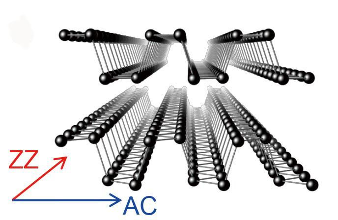
Berkeley Lab researchers have experimentally confirmed strong in-plane anisotropy in thermal conductivity along the zigzag (ZZ) and armchair (AC) directions of single-crystal black phosphorous nanoribbons. Credit: Junqiao Wu, Berkeley Lab
A new experimental revelation about black phosphorus nanoribbons should facilitate the future application of this highly promising material to electronic, optoelectronic and thermoelectric devices. A team of researchers at the U.S. Department of Energy (DOE)'s Lawrence Berkeley National Laboratory (Berkeley Lab) has experimentally confirmed strong in-plane anisotropy in thermal conductivity, up to a factor of two, along the zigzag and armchair directions of single-crystal black phosphorous nanoribbons.
“Imagine the lattice of black phosphorous as a two-dimensional network of balls connected with springs, in which the network is softer along one direction of the plane than another,” says Junqiao Wu, a physicist who holds joint appointments with Berkeley Lab's Materials Sciences Division and the University of California (UC) Berkeley's Department of Materials Science and Engineering.
“Our study shows that in a similar manner heat flow in the black phosphorous nanoribbons can be very different along different directions in the plane. This thermal conductivity anisotropy has been predicted recently for 2D black phosphorous crystals by theorists but never before observed.”
Wu is the corresponding author of a paper describing this research in Nature Communications titled “Anisotropic in-plane thermal conductivity of black phosphorus nanoribbons at temperatures higher than 100K.” The lead authors are Sangwook Lee and Fan Yang. (See below for a complete list of authors)
Black phosphorous, named for its distinctive color, is a natural semiconductor with an energy bandgap that allows its electrical conductance to be switched “on and off.” It has been theorized that in contrast to graphene, black phosphorous has opposite anisotropy in thermal and electrical conductivities – i.e., heat flows more easily along a direction in which electricity flows with more difficultly. Such anisotropy would be a boost for designing energy-efficient transistors and thermoelectric devices, but experimental confirmation proved challenging because of sample preparation and measurement requirements.
“We fabricated black phosphorous nanoribbons in a top-down approach using lithography, then utilized suspended micro-pad devices to thermally isolate the nanoribbons from the environment so that tiny temperature gradient and thermal conduction along a single nanoribbon could be accurately determined,” Wu says. “We also went the extra mile to engineer the interface between the nanoribbon and the contact electrodes to ensure negligible thermal and electrical contact resistances, which is essential for this type of experiment.”
The results of the study, which was carried out at the Molecular Foundry, a DOE Office Science User Facility hosted by Berkeley Lab, revealed high directional anisotropy in thermal conductivity at temperatures greater than 100 Kelvin. This anisotropy was attributed mainly to phonon dispersion with some contribution from phonon-phonon scattering rate, both of which are orientation-dependent.
Detailed analysis revealed that at 300 Kelvin, thermal conductivity decreased as the thickness of the nanoribbon thickness shrank from approximately 300 nanometers to approximately 50 nanometers. The anisotropy ratio remained at a factor of two within this thickness range.
“The anisotropy we discovered in the thermal conductivity of black phosphorous nanoribbons indicates that when these layered materials are patterned into different shapes for microelectronic and optoelectronic devices, the lattice orientation of the patterns should be considered,” Wu says.
“This anisotropy can be especially advantageous if heat generation and dissipation play a role in the device operation. For example, these orientation-dependent thermal conductivities give us opportunities to design microelectronic devices with different lattice orientations for cooling and operating microchips. We could use efficient thermal management to reduce chip temperature and enhance chip performance.”
Wu and his colleagues plan to use their experimental platform to investigate how thermal conductivity in black phosphorous nanoribbons is affected under different scenarios, such as hetero-interfaces, phase-transitions and domain boundaries. They also want to explore the effects of various physical conditions such as stress and pressure.
###
In addition to Wu, Lee and Yang, other co-authors of the Nature Communcations paper are Joonki Suh, Sijie Yang, Yeonbae Lee, Guo Li, Hwan Sung Choe, Aslihan Suslu, Yabin Chen, Changhyun Ko, Joonsuk Park, Kai Liu, Jingbo Li, Kedar Hippalgaonkar, Jeffrey Urban and Sefaattin Tongay.
This research was supported by the DOE Office of Science.
Lawrence Berkeley National Laboratory addresses the world's most urgent scientific challenges by advancing sustainable energy, protecting human health, creating new materials, and revealing the origin and fate of the universe. Founded in 1931, Berkeley Lab's scientific expertise has been recognized with 13 Nobel prizes. The University of California manages Berkeley Lab for the U.S. Department of Energy's Office of Science. For more, visit http://www.
DOE's Office of Science is the single largest supporter of basic research in the physical sciences in the United States, and is working to address some of the most pressing challenges of our time. For more information, please visit the Office of Science website at science.energy.gov/.
Media Contact
All latest news from the category: Materials Sciences
Materials management deals with the research, development, manufacturing and processing of raw and industrial materials. Key aspects here are biological and medical issues, which play an increasingly important role in this field.
innovations-report offers in-depth articles related to the development and application of materials and the structure and properties of new materials.


Newest articles

Properties of new materials for microchips
… can now be measured well. Reseachers of Delft University of Technology demonstrated measuring performance properties of ultrathin silicon membranes. Making ever smaller and more powerful chips requires new ultrathin…

Floating solar’s potential
… to support sustainable development by addressing climate, water, and energy goals holistically. A new study published this week in Nature Energy raises the potential for floating solar photovoltaics (FPV)…

Skyrmions move at record speeds
… a step towards the computing of the future. An international research team led by scientists from the CNRS1 has discovered that the magnetic nanobubbles2 known as skyrmions can be…

