Hybrid pixel array detectors enter the low-noise regime
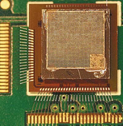
This is a photograph of the JUNGFRAU-0.4 chip and sensor on top of which a 150 µm-thick laser-drilled tungsten mask (Laser Zentrum Hannover eV, Hannover, Germany) with 28 µm-diameter holes is placed. Credit: Jungmann-Smith et al
For decades, detectors have been a limiting factor in experiments at synchrotron radiation facilities. Even though imaging detectors evolved over time, the evolution of the source always outran the evolution of the detector. This situation started to change with the introduction of the so-called hybrid pixel array detectors, which contain a pixelated readout chip custom-designed for a well-defined experiment or technique.
One of the revolutionising advantages offered by this technology is that every single pixel contains all necessary electronics, including for instance counters, for X-ray detection. This massive parallelisation increased the overall efficiency of the detector by several orders of magnitude as compared with the charge-coupled-device-based system.
There are now various examples of HPADs, specifically developed for X-ray experiments at storage-ring synchrotron sources, as well as various spin-off companies commercialising them. Most of these systems are so-called photon-counting detectors, where each incoming photon is processed by the readout electronics in the pixel and individually counted.
The advantage of photon counting is that electronic noise, present in any system, can be efficiently discriminated against, yielding `noise-free' detectors. An application for such low-noise systems is in energy-dispersive measurements.
The researchers show in their paper that, with the use of a proper mask to shield the edge regions between pixels, very good fluorescence spectra can be obtained. This capability was subsequently used for multi-colour imaging at the SOLEIL synchrotron.
The innovative aspect of the work contained in this paper does not lie in the spectroscopic results obtained as they could very well have been obtained with other detectors. But what is truly impressive is that these results were obtained with an HPAD using a standard planar diode array as sensor.
This means that the system uses relatively standard and thus easy-to-manufacture components, making it possible to envision building larger and/or further-optimised systems in the near future. And with that, low-noise HPADs have entered a field formally reserved for silicon drift detectors and complementary metal-oxide semiconductor imagers.
Media Contact
All latest news from the category: Materials Sciences
Materials management deals with the research, development, manufacturing and processing of raw and industrial materials. Key aspects here are biological and medical issues, which play an increasingly important role in this field.
innovations-report offers in-depth articles related to the development and application of materials and the structure and properties of new materials.


Newest articles

Silicon Carbide Innovation Alliance to drive industrial-scale semiconductor work
Known for its ability to withstand extreme environments and high voltages, silicon carbide (SiC) is a semiconducting material made up of silicon and carbon atoms arranged into crystals that is…

New SPECT/CT technique shows impressive biomarker identification
…offers increased access for prostate cancer patients. A novel SPECT/CT acquisition method can accurately detect radiopharmaceutical biodistribution in a convenient manner for prostate cancer patients, opening the door for more…

How 3D printers can give robots a soft touch
Soft skin coverings and touch sensors have emerged as a promising feature for robots that are both safer and more intuitive for human interaction, but they are expensive and difficult…

