GRAPHENE: Growing Giants
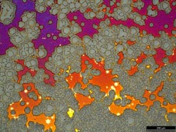
David L. Miller, NIST<br><br>Optical microscope image of a copper film mostly destroyed during graphene growth. What was a continuous copper film has decomposed into grey areas of bare sapphire, rings and irregular patches of copper that appear in a rainbow of colors due to oxidation, and small star-shaped islands of graphene, which appear bright because the graphene protects the copper from oxidation.<br>
To technology insiders, graphene is a certified big deal. The one-atom thick carbon-based material elicits rhapsodic descriptions as the strongest, thinnest material known.
It also is light, flexible, and able to conduct electricity as well as copper. Graphene-based electronics promise advances such as faster internet speeds, cheaper solar cells, novel sensors, space suits spun from graphene yarn, and more.
Now a research team at the National Institute of Standards and Technology (NIST) in Boulder, Colo., may help bring graphene’s promise closer to reality. While searching for an ideal growth platform for the material, investigators developed a promising new recipe for a graphene substrate: a thin film of copper with massive crystalline grains. The team’s findings appear in the journal AIP Advances, which is produced by AIP Publishing.
The key advance is the grain size of the copper substrate. The large grains are several centimeters in size – lunkers by microelectronics standards – but their relative bulk enables them to survive the high temperatures needed for graphene growth, explained NIST researcher Mark Keller.
The inability of most copper films to survive this stage of graphene growth “has been one problem preventing wafer-scale production of graphene devices,” Keller said.
Thin films are an essential component of many electronic, optical, and medical technologies, but the grains in these films are typically smaller than one micrometer. To fabricate the new copper surface, whose grains are about 10,000 times larger, the researchers came up with a two-step process.
First, they deposited copper onto a sapphire wafer held slightly above room temperature. Second, they added the transformative step of annealing, or heat-treating, the film at a much higher temperature, near the melting point of copper. To demonstrate the viability of their giant-grained film, the researchers successfully grew graphene grains 0.2 millimeters in diameter on the new copper surface.
The article, “Giant secondary grain growth in Cu films on sapphire” by David L. Miller, Mark W. Keller, Justin M. Shaw, Katherine P. Rice, Robert R. Keller and Kyle M. Diederichsen appears in the journal AIP Advances. See: http://dx.doi.org/10.1063/1.4817829
ABOUT THE JOURNAL
AIP Advances is a fully open access, online-only, community-led journal. It covers all areas of applied physical science. With its advanced web 2.0 functionality, the journal puts relevant content and discussion tools in the hands of the community to shape the direction of the physical sciences. See: http://aipadvances.aip.org
Media Contact
More Information:
http://www.aip.orgAll latest news from the category: Materials Sciences
Materials management deals with the research, development, manufacturing and processing of raw and industrial materials. Key aspects here are biological and medical issues, which play an increasingly important role in this field.
innovations-report offers in-depth articles related to the development and application of materials and the structure and properties of new materials.


Newest articles

Silicon Carbide Innovation Alliance to drive industrial-scale semiconductor work
Known for its ability to withstand extreme environments and high voltages, silicon carbide (SiC) is a semiconducting material made up of silicon and carbon atoms arranged into crystals that is…

New SPECT/CT technique shows impressive biomarker identification
…offers increased access for prostate cancer patients. A novel SPECT/CT acquisition method can accurately detect radiopharmaceutical biodistribution in a convenient manner for prostate cancer patients, opening the door for more…

How 3D printers can give robots a soft touch
Soft skin coverings and touch sensors have emerged as a promising feature for robots that are both safer and more intuitive for human interaction, but they are expensive and difficult…

