First full colour images at 100,000 dpi resolution
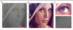
A coloured nanoscale rendition of a standard test image used in image processing experiments - (a) Before the addition of metal in the nanostructures, the image has only grayscale tones as observed under an optical microscope. (b) Colours are observed using the same optical microscope after addition of the metal layers to the nanostrucutres and in specific patterns. (c) Zooming into the image with the same setup, the specular reflection at the corner of the eye is observed showing the refined colour detail that the new method is able to achieve. The region indicated (bottom right) is made up of nanostructures as observed in the electron micrograph.<br><br><br><br>Copyright : Agency for Science, Technology and Research (A*STAR)<br>
Researchers from A*STAR’s Institute of Materials Research and Engineering (IMRE) have developed an innovative method for creating sharp, full-spectrum colour images at 100,000 dots per inch (dpi), using metal-laced nanometer-sized structures, without the need for inks or dyes.
In comparison, current industrial printers such as inkjet and laserjet printers can only achieve up to 10,000 dpi while research grade methods are able to dispense dyes for only single colour images. This novel breakthrough allows colouring to be treated not as an inking matter but as a lithographic matter, which can potentially revolutionise the way images are printed and be further developed for use in high-resolution reflective colour displays as well as high density optical data storage.
The inspiration for the research was derived from stained glass, which is traditionally made by mixing tiny fragments of metal into the glass. It was found that nanoparticles from these metal fragments scattered light passing through the glass to give stained glass its colours. Using a similar concept with the help of modern nanotechnology tools, the researchers precisely patterned metal nanostructures, and designed the surface to reflect the light to achieve the colour images.
“The resolution of printed colour images very much depends on the size and spacing between individual ‘nanodots’ of colour”, explained Dr Karthik Kumar, one of the key researchers involved. “The closer the dots are together and because of their small size, the higher the resolution of the image. With the ability to accurately position these extremely small colour dots, we were able to demonstrate the highest theoretical print colour resolution of 100,000 dpi.”
“Instead of using different dyes for different colours, we encoded colour information into the size and position of tiny metal disks. These disks then interacted with light through the phenomenon of plasmon resonances,” said Dr Joel Yang, the project leader of the research. “The team built a database of colour that corresponded to a specific nanostructure pattern, size and spacing. These nanostructures were then positioned accordingly. Similar to a child’s ‘colouring-by-numbers’ image, the sizes and positions of these nanostructures defined the ‘numbers’. But instead of sequentially colouring each area with a different ink, an ultrathin and uniform metal film was deposited across the entire image causing the ‘encoded’ colours to appear all at once, almost like magic!” added Dr Joel Yang.
The researchers from IMRE had also collaborated with A*STAR’s Institute of High Performance Computing (IHPC) to design the pattern using computer simulation and modelling. Dr Ravi Hegde of IHPC said, “The computer simulations were vital in understanding how the structures gave rise to such rich colours. This knowledge is currently being used to predict the behaviour of more complicated nanostructure arrays.”
The researchers are currently working with Exploit Technologies Pte Ltd (ETPL), A*STAR’s technology transfer arm, to engage potential collaborators and to explore licensing the technology. The research was published online on 12 August 2012 in Nature Nanotechnology, one of the top scientific journals for materials science and nanotechnology.
Encl. Annex A: A*STAR Corporate Profiles
For media enquiries, please contact:
Mr Eugene Low
Manager, Corporate Communications
for Institute of Materials Research and Engineering (IMRE)
3, Research Link
Singapore 117602
DID: +65 6874 8491
Mobile: +65 9230 9235
Email: loweom@scei.a-star.edu.sg
For technical enquiries, please contact:
Dr Karthik Kumar
Scientist I
Institute of Materials Research and Engineering (IMRE)
3, Research Link
Singapore 117602
DID: +65 6872 7743
E-mail: kumark@imre.a-star.edu.sg
Dr Joel Yang
Scientist II
Institute of Materials Research and Engineering (IMRE)
3, Research Link
Singapore 117602
DID: +65 6874 8385
E-mail: yangkwj@imre.a-star.edu.sg
Annex A – A*STAR Corporate Profiles
About the Institute of Materials Research and Engineering (IMRE)
The Institute of Materials Research and Engineering (IMRE) is a research institute of the Agency for Science, Technology and Research (A*STAR). The Institute has capabilities in materials analysis & characterisation, design & growth, patterning & fabrication, and synthesis & integration. We house a range of state-of-the-art equipment for materials research including development, processing and characterisation. IMRE conducts a wide range of research, which includes novel materials for organic solar cells, photovoltaics, printed electronics, catalysis, bio-mimetics, microfluidics, quantum dots, heterostructures, sustainable materials, atom technology, etc. We collaborate actively with other research institutes, universities, public bodies, and a wide spectrum of industrial companies, both globally and locally.
For more information about IMRE, please visit www.imre.a-star.edu.sg
About the Agency for Science, Technology and Research (A*STAR)
The Agency for Science, Technology and Research (A*STAR) is the lead agency for fostering world-class scientific research and talent for a vibrant knowledge-based and innovation-driven Singapore. A*STAR oversees 14 biomedical sciences and physical sciences and engineering research institutes, and six consortia & centres, located in Biopolis and Fusionopolis as well as their immediate vicinity.
A*STAR supports Singapore's key economic clusters by providing intellectual, human and industrial capital to its partners in industry. It also supports extramural research in the universities, hospitals, research centres, and with other local and international partners.
For more information about A*STAR, please visit www.a-star.edu.sg.
Media Contact
All latest news from the category: Materials Sciences
Materials management deals with the research, development, manufacturing and processing of raw and industrial materials. Key aspects here are biological and medical issues, which play an increasingly important role in this field.
innovations-report offers in-depth articles related to the development and application of materials and the structure and properties of new materials.


Newest articles

Properties of new materials for microchips
… can now be measured well. Reseachers of Delft University of Technology demonstrated measuring performance properties of ultrathin silicon membranes. Making ever smaller and more powerful chips requires new ultrathin…

Floating solar’s potential
… to support sustainable development by addressing climate, water, and energy goals holistically. A new study published this week in Nature Energy raises the potential for floating solar photovoltaics (FPV)…

Skyrmions move at record speeds
… a step towards the computing of the future. An international research team led by scientists from the CNRS1 has discovered that the magnetic nanobubbles2 known as skyrmions can be…

