Empa researchers clarify reaction pathway to fabricate graphene-like materials
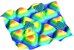
The scanning tunnelling microscope images shows nanographene molecules and the two stabilised intermediate products on a copper surface. The molecular models show a nanographene (at the bottom right) as well as the two intermediate products (above and left). In reality the diameter of the molecule is approximately one nanometre. Photo: Empa<br>
To overcome the current limitations, Empa researchers have fabricated graphene-like materials using a surface chemical route and clarified in detail the corresponding reaction pathway. The work has just been published in the scientific journal “Nature Chemistry“. The scientists combined empirical observations using scanning tunnelling microscopy with computer simulations.
Electronic components are getting smaller and smaller, with microelectronic components gradually being replaced by nanoelectronic ones. On nanoscale dimensions, silicon, which is at the present stage the most commonly used material in semiconductor technology, reaches however a limit, preventing further miniaturization and technological progress. New electronic materials are therefore in great demand. Due to its outstanding electronic properties, graphene, a two-dimensional carbon network, is considered as a possible replacement. However, several obstacles must be overcome before graphene can be used in semiconductor technology. For instance, currently there is no easily applicable method for large-scale processing of graphene-like materials.
Empa researchers of the nanotech@surfaces Laboratory reported on a surface chemical route to fabricate small fragments of graphene, so-called nanographenes. Using a prototypical polyphenylene precursor, the researchers clarified, together with scientists at the Max Planck Institute for Polymer Research in Mainz (Germany) and the University of Zurich, how the reaction pathway runs in detail on a copper surface und how the building blocks can be transformed into planar nanographenes directly on the surface. The work has been published last Sunday in the scientific journal “Nature Chemistry” as an advanced online publication.
Successful partners: experiment and simulation
For their investigations the researchers combined empirical observations, in particular from scanning tunnelling microscopy with computer simulations. The simulations are used to determine whether a theoretically possible reaction step is energetically possible or not. The result: the reaction pathway consists of six steps with five intermediate products. Two of them are stabilised by the surface so that they can be stably imaged with the scanning tunnelling microscope. The reaction barriers connecting the different intermediates are lowered through a catalytic effect of the substrate.
To be capable of being integrated in electronic circuits, the graphene-like material must however be manufactured on semiconductor surfaces instead of metal ones. The researchers have simulated whether their approach could also work on these surfaces and the results are very promising, showing that surface-supported synthesis is a possible way to fabricate tailored nanographenes on a range of different substrates.
The three pillars of today’s science: theory, experiment, and simulation
Progress in today’s scientific research relies at the same time on theory, experiments, and to an increasing extent on computer simulations. These simulations are complementary to often complex lab experiments and make it possible to get further information that cannot be obtained with experimental methods alone. The combination of experiments and simulations as well as the deduced theories therefore allow for a more and more accurate explanation and precise prediction of natural phenomena.
Literature reference
“Surface-assisted cyclodehydrogenation provides a synthetic route towards easily processable and chemically tailored nanographenes”, M. Treier, C.A. Pignedoli, T. Laino, R. Rieger, K. Müllen, D. Passerone, R. Fasel, Nature Chemistry, published online 7 November 2010; DOI: 10.1038/NCHEM.891
Media Contact
More Information:
http://www.empa.chAll latest news from the category: Materials Sciences
Materials management deals with the research, development, manufacturing and processing of raw and industrial materials. Key aspects here are biological and medical issues, which play an increasingly important role in this field.
innovations-report offers in-depth articles related to the development and application of materials and the structure and properties of new materials.


Newest articles

Superradiant atoms could push the boundaries of how precisely time can be measured
Superradiant atoms can help us measure time more precisely than ever. In a new study, researchers from the University of Copenhagen present a new method for measuring the time interval,…

Ion thermoelectric conversion devices for near room temperature
The electrode sheet of the thermoelectric device consists of ionic hydrogel, which is sandwiched between the electrodes to form, and the Prussian blue on the electrode undergoes a redox reaction…

Zap Energy achieves 37-million-degree temperatures in a compact device
New publication reports record electron temperatures for a small-scale, sheared-flow-stabilized Z-pinch fusion device. In the nine decades since humans first produced fusion reactions, only a few fusion technologies have demonstrated…

