Edgy Look at 2D Molybdenum Disulfide
A new SHG imaging technique allows rapid and all-optical determination of the crystal orientations of 2D semiconductor membranes at a large scale, providing the knowledge needed to use these materials in nanoelectronic devices.
The drive to develop ultrasmall and ultrafast electronic devices using a single atomic layer of semiconductors, such as transition metal dichalcogenides, has received a significant boost. Researchers with the U.S. Department of Energy (DOE)’s Lawrence Berkeley National Laboratory (Berkeley Lab) have recorded the first observations of a strong nonlinear optical resonance along the edges of a single layer of molybdenum disulfide.
The existence of these edge states is key to the use of molybdenum disulfide in nanoelectronics, as well as a catalyst for the hydrogen evolution reaction in fuel cells, desulfurization and other chemical reactions.
“We observed strong nonlinear optical resonances at the edges of a two-dimensional crystal of molybdenum disulfide” says Xiang Zhang, a faculty scientist with Berkeley Lab’s Materials Sciences Division who led this study. “These one-dimensional edge states are the result of electronic structure changes and may enable novel nanoelectronics and photonic devices.
These edges have also long been suspected to be the active sites for the electrocatalytic hydrogen evolution reaction in energy applications. We also discovered extraordinary second harmonic light generation properties that may be used for the in situ monitoring of electronic changes and chemical reactions that occur at the one-dimensional atomic edges.”
Zhang, who also holds the Ernest S. Kuh Endowed Chair Professor at the University of California (UC) Berkeley and directs the National Science Foundation’s Nano-scale Science and Engineering Center, is the corresponding author of a paper in Science describing this research. The paper is titled “Edge Nonlinear Optics on a MoS2 Atomic Monolayer.” Co-authors are Xiaobo Yin, Ziliang Ye, Daniel Chenet, Yu Ye, Kevin O’Brien and James Hone.
Emerging two-dimensional semiconductors are prized in the electronics industry for their superior energy efficiency and capacity to carry much higher current densities than silicon. Only a single molecule thick, they are well-suited for integrated optoelectronic devices.
Until recently, graphene has been the unchallenged superstar of 2D materials, but today there is considerable attention focused on 2D semiconducting crystals that consist of a single layer of transition metal atoms, such as molybdenum, tungsten or niobium, sandwiched between two layers of chalcogen atoms, such as sulfur or selenium. Featuring the same flat hexagonal “honeycombed” structure as graphene and many of the same electrical advantages, these transition metal dichalcogenides, unlike graphene, have direct energy bandgaps. This facilitates their application in transistors and other electronic devices, particularly light-emitting diodes.
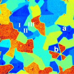
Full realization of the vast potential of transition metal dichalcogenides will only come with a better understanding of the domain orientations of their crystal structures that give rise to their exceptional properties. Until now, however, experimental imaging of these three-atom-thick structures and their edges have been limited to scanning tunneling microscopy and transmission electron microscopy, technologies that are often difficult to use. Nonlinear optics at the crystal edges and boundaries enabled Zhang and his collaborators to develop a new imaging technique based on second-harmonic generation (SHG) light emissions that can easily capture the crystal structures and grain orientations with an optical microscope.
“Our nonlinear optical imaging technique is a non-invasive, fast, easy metrologic approach to the study of 2D atomic materials,” says Xiaobo Yin, the lead author of the Science paper and a former member of Zhang’s research group who is now on the faculty at the University of Colorado, Boulder. “We don’t need to prepare the sample on any special substrate or vacuum environment, and the measurement won’t perturb the sample during the imaging process. This advantage allows for in-situ measurements under many practical conditions. Furthermore, our imaging technique is an ultrafast measurement that can provide critical dynamic information, and its instrumentation is far less complicated and less expensive compared with scanning tunneling microscopy and transmission electron microscopy.”
For the SHG imaging of molybdenum disulfide, Zhang and his collaborators illuminated sample membranes that are only three atoms thick with ultrafast pulses of infrared light. The nonlinear optical properties of the samples yielded a strong SHG response in the form of visible light that is both tunable and coherent. The resulting SHG-generated images enabled the researchers to detect “structural discontinuities” or edges along the 2D crystals only a few atoms wide where the translational symmetry of the crystal was broken.
“By analyzing the polarized components of the SHG signals, we were able to map the crystal orientation of the molybdenum disulfide atomic membrane,” says Ziliang Ye, the co-lead author of the paper and current member of Zhang’s research group. “This allowed us to capture a complete map of the crystal grain structures, color-coded according to crystal orientation. We now have a real-time, non-invasive tool that allows us explore the structural, optical, and electronic properties of 2D atomic layers of transition metal dichalcogenides over a large area.”
This research was supported by the DOE Office of Science through the Energy Frontier Research Center program, and by the U.S. Air Force Office of Scientific Research Multidisciplinary University Research Initiative.
Additional Information
For more about the research of Xiang Zhang go here
Xiang Zhang can be reached for comment at (Mobile): 510-225-8559510-225-8559). Xiaobo Yin can be reached at 650-796-3276650-796-3276 and Ziliang Ye at 510-508-6128
510-508-6128.
# # #
Lawrence Berkeley National Laboratory addresses the world’s most urgent scientific challenges by advancing sustainable energy, protecting human health, creating new materials, and revealing the origin and fate of the universe. Founded in 1931, Berkeley Lab’s scientific expertise has been recognized with 13 Nobel prizes. The University of California manages Berkeley Lab for the U.S. Department of Energy’s Office of Science. For more, visit www.lbl.gov.
The DOE Office of Science is the single largest supporter of basic research in the physical sciences in the United States and is working to address some of the most pressing challenges of our time. For more information, please visit science.energy.gov.
Media Contact
All latest news from the category: Materials Sciences
Materials management deals with the research, development, manufacturing and processing of raw and industrial materials. Key aspects here are biological and medical issues, which play an increasingly important role in this field.
innovations-report offers in-depth articles related to the development and application of materials and the structure and properties of new materials.


Newest articles

Silicon Carbide Innovation Alliance to drive industrial-scale semiconductor work
Known for its ability to withstand extreme environments and high voltages, silicon carbide (SiC) is a semiconducting material made up of silicon and carbon atoms arranged into crystals that is…

New SPECT/CT technique shows impressive biomarker identification
…offers increased access for prostate cancer patients. A novel SPECT/CT acquisition method can accurately detect radiopharmaceutical biodistribution in a convenient manner for prostate cancer patients, opening the door for more…

How 3D printers can give robots a soft touch
Soft skin coverings and touch sensors have emerged as a promising feature for robots that are both safer and more intuitive for human interaction, but they are expensive and difficult…

