Cutting the graphene cake

Writing in Nature Materials, the scientists show that a new side-view imaging technique can be used to visualize the individual atomic layers of graphene within the devices they have built. They found that the structures were almost perfect even when more than 10 different layers were used to build the stack.
This surprising result indicates that the latest techniques of isolating graphene could be a huge leap forward for engineering at the atomic level.
This development gives more weight to graphene's suitability as a major component in the next generation of computer chips.
The researchers' side-view imaging approach works by first extracting a thin slice from the centre of the device. This is similar to cutting through a rock to reveal the geological layers or slicing into a chocolate gateaux to reveal the individual layers of icing.
The scientists used a beam of ions to cut into the surface of the graphene and dig a trench on either side of the section they wanted to isolate. They then removed a thin slice of the device. Wonder material graphene is a two dimensional material consisting of a single layer of carbon atoms arranged in a honeycomb or chicken wire structure. It is the thinnest material in the world and yet is also one of the strongest. It conducts electricity as efficiently as copper and outperforms all other materials as a conductor of heat.
Demonstrating its remarkable properties won Professor Andre Geim and Professor Kostya Novoselov the Nobel prize for Physics in 2010. The University of Manchester is building a state-of-the-art National Graphene Institute to continue to lead the way in graphene research.
Dr Sarah Haigh, from The University of Manchester's School of Materials, said: “The difference is that our slices are only around 100 atoms thick and this allows us to visualize the individual atomic layers of graphene in projection.
“We have found that the observed roughness of the graphene is correlated with their conductivity. Of course we have to make all our electrical measurements before cutting into the device. We were also able to observe that the layers were perfectly clean and that any debris left over from production segregated into isolated pockets and so did not affect device performance.
“We plan to use this new side view imaging approach to improve the performance of our graphene devices.”
Media Contact
More Information:
http://www.manchester.ac.ukAll latest news from the category: Materials Sciences
Materials management deals with the research, development, manufacturing and processing of raw and industrial materials. Key aspects here are biological and medical issues, which play an increasingly important role in this field.
innovations-report offers in-depth articles related to the development and application of materials and the structure and properties of new materials.
Newest articles

Properties of new materials for microchips
… can now be measured well. Reseachers of Delft University of Technology demonstrated measuring performance properties of ultrathin silicon membranes. Making ever smaller and more powerful chips requires new ultrathin…

Floating solar’s potential
… to support sustainable development by addressing climate, water, and energy goals holistically. A new study published this week in Nature Energy raises the potential for floating solar photovoltaics (FPV)…

Skyrmions move at record speeds
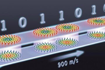
… a step towards the computing of the future. An international research team led by scientists from the CNRS1 has discovered that the magnetic nanobubbles2 known as skyrmions can be…


