New chemical method paves the way for making a greater variety of light-sensitive materials that was not possible before
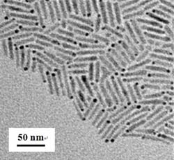
Metal-semiconductor ‘matchstick-like’ structures viewed under high-powered transmission electron microscopy. Copyright : IMRE <br>
Scientists from Singapore’s Institute of Materials Research and Engineering (IMRE) and National University of Singapore (NUS) have created a new chemical method that enables the development of a variety of tiny light conducting metal-semiconductor contacts. These light-sensitive nano-sized components could help create bioimaging labels as well as better photocatalysts used in fuel cells.
1. Sticking a ball onto a small pole might seem simple but try doing that at a scale a billion times smaller. Researchers have been making ‘matchstick-like’ nano-sized metal ball-semiconductor pole features with light-sensitive properties for some time but with great difficulty and strict limitations on the type of metals that can be used. The ‘matchstick-like’ shape is used because the ends of a semiconductor pole have been found to be more chemically reactive compared to other shapes thus allowing metals to be deposited easier. Scientists from IMRE and NUS have recently discovered a chemical process that is not only simpler to perform but greatly expands the range of different metals that can be coupled with the semiconductors. This opens the way for nano-sized structures with enhanced photoconductive properties or with entirely new functions. For example, the new nanostructures chemically synthesised by the researchers may be further developed as labels for enhanced bio-imaging applications such as magnetic resonance imaging (MRI), fluorescence and dark field imaging.
2. Referring to the possibility of the nanostructures being used to enhance current bioimaging techniques, Dr Chan Yin Thai, an IMRE scientist, explained, “The breakthrough may allow multiple imaging modes to be supported by a single label, which can significantly improve current imaging capabilities and give rise to powerful diagnostic tools”.
3. The light-sensitive metal-semiconductor pole features also have intrinsically good photocatalytic properties, where chemical reactions are triggered by light. For the moment, the researchers are looking at using the new method to produce materials that have ‘green’ photocatalytic applications, for instance, materials that enhance water-splitting to produce hydrogen more efficiently for fuel cells; and materials that actively degrade environmental pollutants on exposed surfaces like buildings and cars.
4. “The development of metal-semiconductor nanostructures for use in devices is still in its infancy but having access to a large variety of different metals really opens doors to a vast number of possibilities for scientific exploration and is a crucial milestone for ensuring continued R&D,” Dr Chan explained.
5. The scientists used a novel approach to develop the new method – by exploiting the light-sensitive properties of the semiconductor ‘pole’. By putting gold particles onto the ‘pole’ and then treating it with UV light, the IMRE and NUS scientists discovered that this made it easier to attach a greater variety of metals, using only mild chemicals. Before the success of this research, the metals that could be used for the ‘ball’ were limited. The chemicals needed in conventional treatment had to be mild so that it would not degrade the semiconductor ‘pole’. The degradation of the ‘pole’ would affect the photocatalytic properties of the structure. This limited the variety of metals that could be used as tougher metals could not be fixed onto the ‘pole’ using the mild chemicals.
6. The research paper, “Light-Induced Selective Deposition of Metals on Gold-Tipped CdSe-Seeded CdS Nanorods” was recently published in the well-known Journal of the American Chemical Society.
For media enquiries, please contact:
Mr Eugene Low
Manager, Corporate Communications
for Institute of Materials Research and Engineering (IMRE)
3, Research Link
Singapore 117602
DID: +65 6874 8491
Mobile: +65 9230 9235
Email: loweom(at)scei.a-star.edu.sg
For technical enquiries, please contact:
Dr Chan Yin Thai
Scientist III
3, Research Link
Singapore 117602
DID: +65 6874 8363
Email: chanyt(at)scei.a-star.edu.sg
A*STAR Corporate Profiles:
About the Institute of Materials Research and Engineering (IMRE)
The Institute of Materials Research and Engineering (IMRE) is a research institute of the Agency for Science, Technology and Research (A*STAR). The Institute has capabilities in materials analysis & characterisation, design & growth, patterning & fabrication, and synthesis & integration. We house a range of state-of-the-art equipment for materials research including development, processing and characterisation. IMRE conducts a wide range of research, which includes novel materials for organic solar cells, photovoltaics, printed electronics, catalysis, bio-mimetics, microfluidics, quantum dots, heterostructures, sustainable materials, atom technology, etc. We collaborate actively with other research institutes, universities, public bodies, and a wide spectrum of industrial companies, both globally and locally. For more information about IMRE, please see the links below.
About the Agency for Science, Technology and Research (A*STAR)
The Agency for Science, Technology and Research (A*STAR) is the lead agency for fostering world-class scientific research and talent for a vibrant knowledge-based and innovation-driven Singapore. A*STAR oversees 14 biomedical sciences and physical sciences and engineering research institutes, and six consortia & centres, located in Biopolis and Fusionopolis as well as their immediate vicinity. A*STAR supports Singapore's key economic clusters by providing intellectual, human and industrial capital to its partners in industry. It also supports extramural research in the universities, hospitals, research centres, and with other local and international partners. For more information about A*STAR, please see the links below.
Journalists can request copies of the research paper from r.bisson(at)researchsea.com.
Media Contact
All latest news from the category: Materials Sciences
Materials management deals with the research, development, manufacturing and processing of raw and industrial materials. Key aspects here are biological and medical issues, which play an increasingly important role in this field.
innovations-report offers in-depth articles related to the development and application of materials and the structure and properties of new materials.


Newest articles
“Nanostitches” enable lighter and tougher composite materials
In research that may lead to next-generation airplanes and spacecraft, MIT engineers used carbon nanotubes to prevent cracking in multilayered composites. To save on fuel and reduce aircraft emissions, engineers…
Trash to treasure
Researchers turn metal waste into catalyst for hydrogen. Scientists have found a way to transform metal waste into a highly efficient catalyst to make hydrogen from water, a discovery that…
Real-time detection of infectious disease viruses
… by searching for molecular fingerprinting. A research team consisting of Professor Kyoung-Duck Park and Taeyoung Moon and Huitae Joo, PhD candidates, from the Department of Physics at Pohang University…

